
Selective Soldering Process Optimization
By:PCBBUY 05/29/2026 14:49
Improving Through-Hole Solder Joint Quality in Modern PCB Assembly
As electronic products become increasingly compact and mixed-technology, traditional wave soldering is no longer suitable for many assemblies. Selective soldering has emerged as a critical solution for through-hole components that cannot tolerate full wave exposure.
However, achieving stable and repeatable results requires systematic selective soldering process optimization.
At PCBBUY, selective soldering is not treated as a standalone operation, but as a controlled, data-driven process integrated with PCB design, SMT reflow, and final inspection—ensuring high solder joint reliability for complex assemblies.
What Is Selective Soldering?
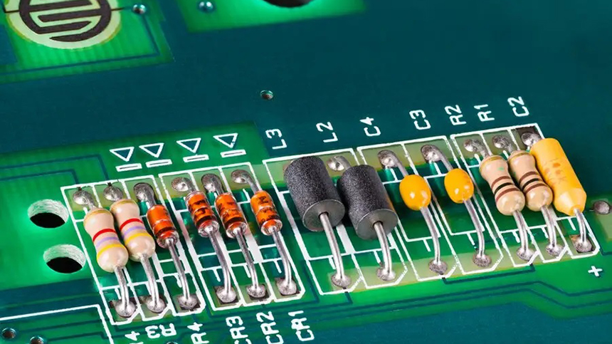
Selective soldering is a soldering process that uses a localized solder fountain or mini-wave to solder specific through-hole joints while protecting nearby SMT components.
It is widely used for:
-
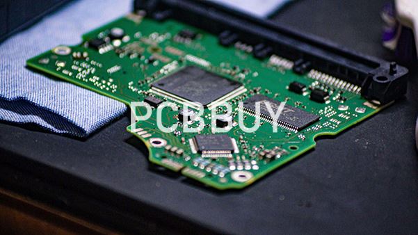
Mixed SMT + THT assemblies
-
Heat-sensitive components
-
High-density PCBs with limited keep-out areas
-
Connectors, transformers, and power devices
Selective soldering process optimization focuses on controlling all variables that influence solder joint quality, repeatability, and yield.
Why Selective Soldering Process Optimization Is Necessary?
Without proper optimization, selective soldering may lead to:
-
Insufficient hole fill
-
Bridging or solder balls
-
Cold joints or dewetting
-
Flux residue and contamination
-
Thermal damage to nearby components
Optimized selective soldering ensures:
-
Consistent hole fill and fillet formation
-
Stable wetting on plated through-holes
-
Minimal thermal stress
-
High first-pass yield
This is especially important for industrial, automotive, and power electronics.
Key Parameters in Selective Soldering Process Optimization
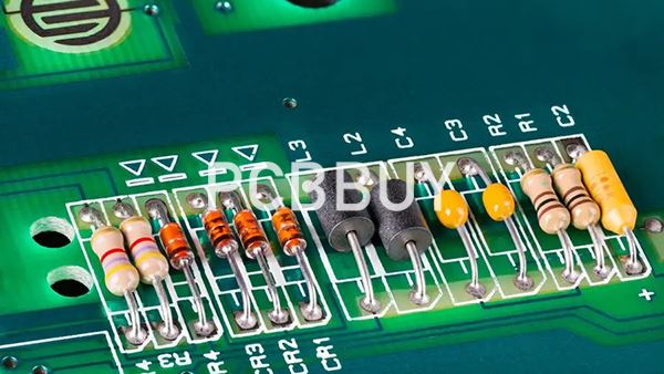
Selective soldering quality depends on multiple interrelated parameters:
-
Flux type and application volume
-
Preheating temperature and uniformity
-
Solder alloy composition
-
Nozzle size and wave stability
-
Dwell time and contact angle
-
PCB finish and hole copper thickness
PCBBUY applies closed-loop process control to maintain consistency across prototype and mass production.
PCBBUY Selective Soldering Process Optimization Capabilities
The following table summarizes how PCBBUY optimizes selective soldering processes at each critical stage:
|
Process Stage |
Optimization Focus |
Technical Purpose |
PCBBUY Capability |
|
Flux Application |
Precise spray & micro-drop control |
Improve wetting, reduce residue |
Programmable fluxing systems |
|
Preheating |
Controlled top & bottom heating |
Activate flux, prevent thermal shock |
Multi-zone infrared & convection preheaters |
|
Solder Alloy Selection |
Lead-free / high-reliability alloys |
Match application requirements |
SAC305, SnCu, SnPb support |
|
Nozzle Design |
Single / multi-nozzle selection |
Prevent bridging, improve access |
Interchangeable nozzle systems |
|
Dwell Time Control |
Contact time optimization |
Ensure full hole fill |
Recipe-based parameter control |
|
PCB Finish Matching |
ENIG / OSP / HASL compatibility |
Improve solderability |
Process tuning per surface finish |
|
Process Monitoring |
Temperature & wave stability |
Maintain repeatability |
SPC-based monitoring |
|
Post-Solder Inspection |
AOI & visual inspection |
Verify joint quality |
Integrated inspection workflow |
Design and PCB Factors Affecting Selective Soldering Results
Selective soldering process optimization begins before assembly, at the PCB design and fabrication stage:
-
Proper pad and hole size design
-
Adequate annular ring and copper thickness
-
Compatible surface finish selection
-
Sufficient keep-out distance from SMT parts
-
Controlled board thickness and flatness
PCBBUY supports DFM review and manufacturability feedback to ensure selective soldering success from the start.

Typical Applications for Optimized Selective Soldering
Selective soldering with optimized parameters is commonly required for:
-
Industrial control boards
-
Automotive power and signal modules
-
Communication equipment
-
Power supplies and converters
-
Medical electronics
PCBBUY supports both low-volume prototypes and high-mix, mid-to-high volume production with consistent process control.
FAQ
What is selective soldering process optimization?
It is the systematic adjustment and control of fluxing, preheating, solder wave, and timing parameters to achieve stable, high-quality through-hole solder joints.
How is selective soldering different from wave soldering?
Selective soldering targets only specific joints using localized solder contact, while wave soldering exposes the entire PCB to a solder wave.
Why is flux control important in selective soldering?
Excess flux can cause residue and contamination, while insufficient flux leads to poor wetting. Optimized flux volume ensures clean and reliable joints.
Does PCB surface finish affect selective soldering quality?
Yes. ENIG, OSP, and HASL behave differently during soldering. PCBBUY adjusts parameters based on surface finish to ensure consistent results.
Can selective soldering be used for lead-free assemblies?
Yes. PCBBUY supports lead-free selective soldering with optimized temperature profiles and SAC-based alloys.
Is selective soldering suitable for high-density PCBs?
Yes, when properly optimized. Nozzle selection, dwell time, and keep-out design are critical for dense layouts.
Conclusion
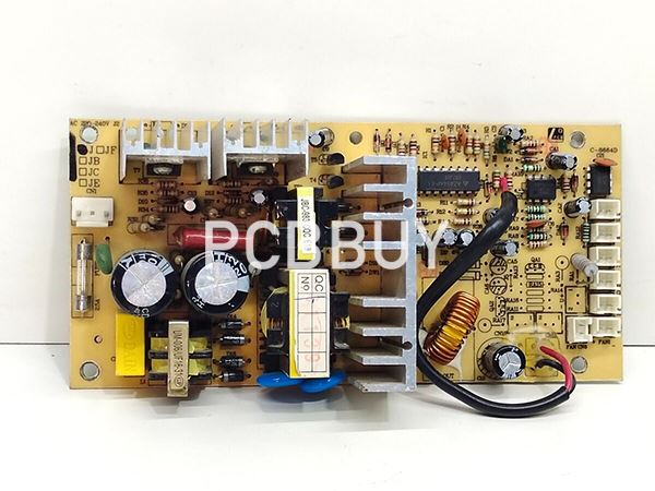
Selective soldering process optimization is essential for achieving reliable through-hole solder joints in today’s mixed-technology PCB assemblies.
Through precise parameter control, advanced equipment, and integrated inspection, PCBBUY delivers stable selective soldering performance from design validation to volume production.
For manufacturers seeking high reliability, minimal rework, and consistent quality, selective soldering optimization is not optional—it is a competitive advantage.
Industry Category








