Simply Explain PCB Copper to Edge Clearance
By:PCBBUY 12/25/2025 16:17

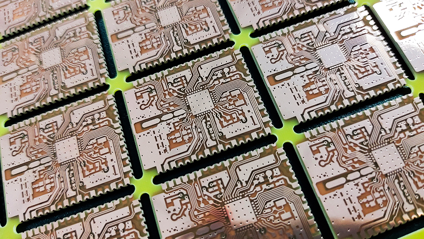
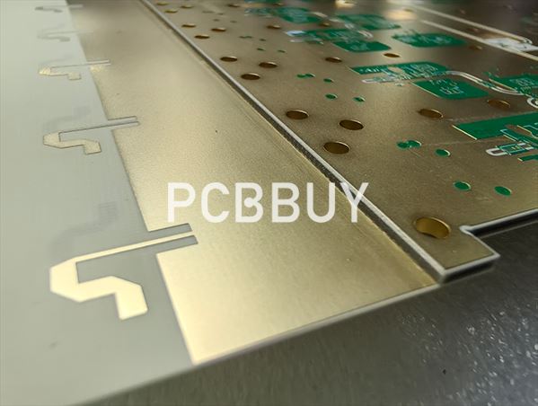
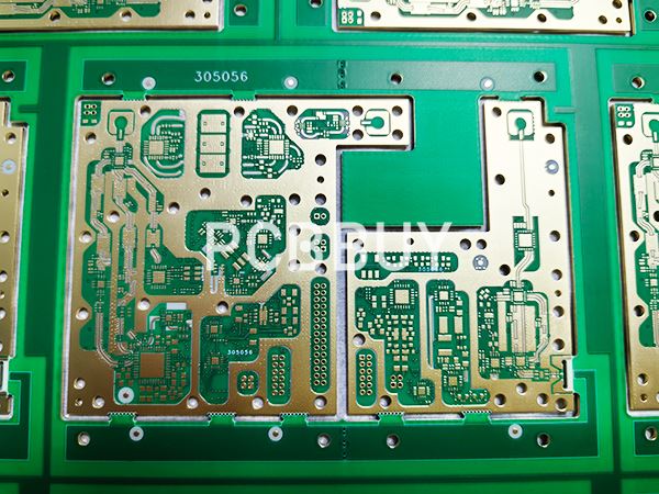
PCB copper to edge clearance refers to the minimum distance between any copper feature—such as traces, pads, copper pours, or vias—and the physical edge of the PCB.
This clearance is a critical parameter in both PCB design and manufacturing, as it directly affects electrical safety, mechanical integrity, and compliance with IPC guidelines.
That’s why copper to edge clearance is a basic but very important rule in PCB design.
Why Copper to Edge Clearance Is Important?
Maintaining proper copper to edge clearance is essential for several reasons:
-
Electrical safety: Prevents short circuits, arcing, or breakdown at the board edge
-
Mechanical reliability: Reduces the risk of copper damage during routing or V-cut
-
Manufacturing yield: Minimizes defects such as exposed copper or edge burrs
-
Standards compliance: Helps designs align with IPC design guidelines
For industrial, automotive, or high-voltage PCBs, insufficient clearance can lead to serious reliability issues.

IPC Guidelines for Copper to Edge Clearance
IPC standards such as IPC-2221 provide design guidance for copper to edge clearance based on:
-
Product application
-
Voltage requirements
-
Manufacturing tolerances
Instead of fixed values, IPC encourages designers to leave enough margin to ensure safe and reliable production.
What Affects the Required Clearance?
Copper to edge clearance depends on several factors:
-
PCB depanelization method
-
Copper thickness
-
Board structure (single, multilayer, HDI)
-
Operating environment
Understanding these factors helps avoid unnecessary production issues.

How PCBBUY Supports Proper Copper to Edge Clearance?
PCBBUY helps customers by:
-
Checking copper to edge clearance during DFM review
-
Using reliable edge routing and depanelization processes
-
Communicating design risks before production starts
This proactive approach helps improve yield and reduce delays.
When Should You Increase Copper to Edge Clearance?
You should consider larger clearance if your PCB is used for:
-
High-voltage applications
-
Industrial or automotive electronics
-
Thick copper or high-reliability designs
PCBBUY engineers are available to review your design and provide guidance.

Why Choose PCBBUY?
With strong engineering support and extensive export experience, PCBBUY is a reliable partner for IPC-compliant PCB manufacturing.
Conclusion
PCB copper to edge clearance is a small design detail with a significant impact on safety and reliability.
With IPC-based guidelines and strong process control, PCBBUY ensures consistent, high-quality PCB manufacturing for global customers.
What is PCB copper to edge clearance?
It is the minimum distance between any copper feature and the physical edge of a PCB.
What IPC standard applies to copper to edge clearance?
IPC-2221 provides general design guidance for PCB copper to edge clearance.
Why is copper to edge clearance important?
It prevents copper exposure, electrical shorts, and mechanical damage during manufacturing and use.
What happens if copper is too close to the PCB edge?
Copper may be damaged during routing or depanelization, leading to exposed copper or electrical failure.
Can PCBBUY help review copper to edge clearance?
Yes. PCBBUY performs DFM reviews and provides engineering advice based on IPC guidelines and manufacturing capability.
Industry Category


