Standard PCB Size: How to Determine in PCB Manufacturing?
By:PCBBUY 03/25/2022 10:23

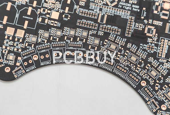
Let’s define exactly what a “pad” is. A pad, also known as a “land,” is the exposed area of metal on a circuit board that the lead of a part will be soldered to. Multiple pads are used to create the component footprint, or land pattern, on the printed circuit board.
This process could be very error-prone, however, as manufacturers’ specifications didn’t always adhere to the same formulas. This could result in layout designers using the wrong sizes and shapes in their pads. In this passage, we are providing all the information of standard PCB size, please check and read the content below.

The standard of PCB pad size
Here are the design standards of PCB Pad shape and size:
The PCB Standard Packaging Library should be used.
· All pads should have a minimum of 0.25mm unilateral and a maximum total pad diameter not greater than 3 times the aperture of the part.
· It is important to ensure that the distance between the two pads is greater than 0.4mm. In the case of dense wiring, the recommended oval and oval plate. Single-panel pad diameter or minimum width of 1.6mm; weak-sided double-sided circuit board pad diameter hole diameter plus 0.5mm can be too large pad easily lead to unnecessary welding.
· Pads with a hole diameter of more than 1.2 mm or with a pad diameter of more than 3.0 mm should be designed as diamond or plummet pads
· For the plug-in components, in order to avoid the phenomenon of copper foil broken when welding, and the single side of the copper foil with a completely coated; and double-sided minimum requirements should make up the tear drop.
Standard PCB Panel Size
We cannot discuss the standard PCB panel size without mentioning the thickness of a circuit board. It is essential to manufacture a circuit board, and if the consistency is not measured correctly, the PCB will not function well if it even functions at all.
As a customer who intends to buy a perfect PCB, you should say where and how the PCB you want to buy will be used. This information will go a long way to help makers decide how thick the circuit board will be. If you're going to buy more than one PCB, you should also tell your producers the different devices you want each type to work with. This way, the level of thickness for every PCB you get will vary concerning the intended function of the electronic device.
By standard PCB panel size, the thickness of an average circuit board is 0.063inches. To achieve maximum efficiency of a PCB, this size and other preparation steps are put into consideration. The standard PCB panel size is calculated so that a highly efficient utilization area utilization is achieved.

Standard PCB Core Sizes
A design specification that impacts your stackup layer and overall board thickness is your choice for core size. The PCB core, along with substrate, prepreg and laminate refers to basic material sections within your board’s construction. The core differs from a substrate in that a substrate has copper attached on one side while the core has copper on both sides. Additionally, all PCBs have a core, even single-layer boards. Depending upon your PCB thickness, you may opt to use one of the commonly used or PCB standard core sizes that range from 0.005 to 0.039 in (.0127 to 1 mm). It is also advisable not to use prepreg dielectric layer thickness below 3 mil. Also, you are better served by choosing 2-ply for prepreg layers.
Knowing standard PCB sizes for the board parameters discussed above can aid you in designing boards that can be readily built with a high yield rate, especially if you consult with your CM to ensure manufacturing regulations and DFM guidelines are adhered to. At Tempo Automation, the industry leader for fast, high-quality PCBA prototypes and low-volume manufacturing, we will work with you from Day 1 of design to ensure that your boards incorporate your design intent and are first-time right manufacturable.
What are the advantages of PCB panel?
The maximum benefit size or PCB size varies depending on the PCB manufacturer and technical equipment. Based on the standard PCB panel size cut 610 * 530mm, which is often processed, there are maximum dimensions of approx. 570 * 490mm for many manufacturers. In electronics production at CAD-UL, the maximum dimensions are specified by the machines used, provided that it is to be carried out completely mechanically:
· Paste printer 600 * 600mm
· SMD pick and place machine 400 * 550mm
· Vapor phase soldering system 550 * 600mm
The following reasons speak against the processing of benefits with the maximum dimensions:
As PCB panel size increases, this also loses stability, which can also be seen depending on the PCB thickness. There is a risk that the connection points between the circuit boards break due to improper handling.

The base materials for printed circuit boards can shrink or stretch during the printed circuit board manufacturing process (dimensional stability). In addition, there are of course manufacturing tolerances in the production process of the circuit board, which can lead to an offset of copper structuring, to drilling and contour of the circuit board and to an offset from layer to layer. With a lot of know-how and by adapting the production data, the PCB manufacturers manage to keep the effects to a minimum. With very large circuit boards or with large benefits where components with small pads, e.g. B. 0.4mm pitch, placed far apart, this can lead to borderline differences between the x, y positions of the pads on the circuit boards and the associated breakouts of the steel stencils for paste printing.
Industry Category


