
TGV vs Microvia for Advanced PCB Interconnects: What Is the Difference?
By:PCBBUY 09/30/2026 15:25
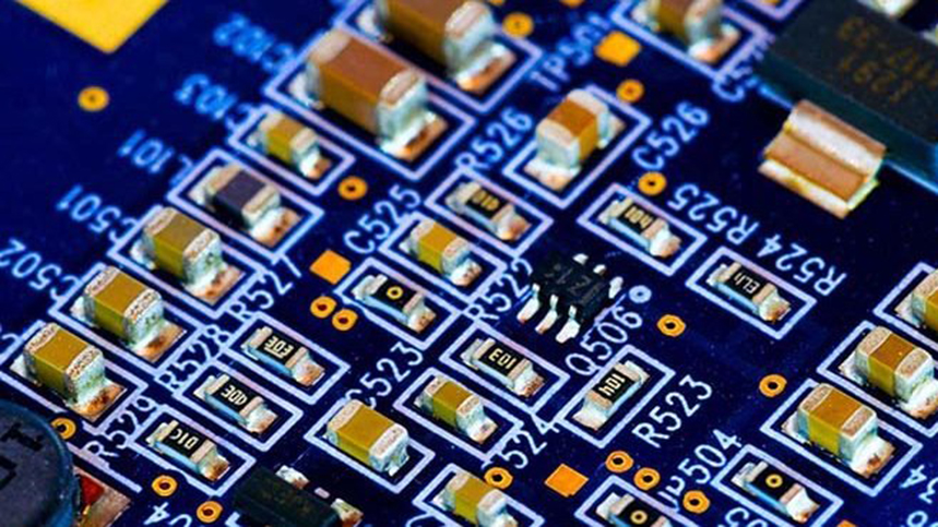
As electronic systems become smaller and more highly integrated, vertical interconnection technologies are becoming increasingly important. TGV vs microvia for advanced PCB interconnects is therefore a topic that often arises when engineers evaluate high-density substrates, advanced packaging structures, and next-generation interconnection solutions.
However, TGVs and microvias are not simply two competing versions of the same technology.
A conventional microvia is generally associated with HDI PCB structures and connects adjacent or selected dielectric layers, while a TGV, or Through-Glass Via, passes through a glass substrate and is more commonly associated with glass interposers and advanced packaging.
The right choice depends on the substrate, interconnection architecture, electrical requirements, mechanical constraints, and manufacturing process. For PCB applications, a well-controlled HDI microvia structure can provide a practical route to higher routing density without unnecessarily introducing the process complexity of a glass interposer.
What Is a Microvia?
A microvia is a small-diameter blind or buried via formed in a dielectric layer, typically using laser drilling in HDI PCB manufacturing. Unlike a conventional mechanically drilled through-hole, a microvia generally has a much shorter vertical interconnection path.
This structure provides several important design advantages:
-
More efficient layer-to-layer interconnection
-
Greater routing density
-
Reduced via footprint
-
More flexible escape routing for fine-pitch components
-
Shorter electrical interconnection paths
Microvias are particularly useful when PCB designers need to route densely populated component areas while controlling the number of PCB layers.
For example, first-order and second-order HDI structures can be used to build sequential interconnections between selected layers. The actual microvia geometry should be determined from the dielectric thickness, pad size, aspect ratio, laser process window, copper formation process, and reliability requirements rather than simply choosing the smallest possible via.

What Is a TGV?
A TGV, or Through-Glass Via, is a vertical conductive interconnection formed through a glass substrate. Unlike a PCB microvia, which is normally formed within a dielectric layer of an HDI board, a TGV extends through the thickness of a glass substrate.
Glass substrates are being investigated for advanced packaging and interposer applications because of characteristics such as high flatness, dimensional stability, electrical insulation, and the possibility of large-panel processing. TGVs can provide vertical electrical connections between metallization structures on different sides of the glass substrate.
TGV fabrication can involve specialized laser-based glass processing and subsequent metallization. Because glass is electrically insulating, the via must be metallized to create the conductive path. This introduces process considerations that differ substantially from conventional organic PCB microvia manufacturing.
TGV vs Microvia: Basic Structural Comparison
|
Factor |
Microvia |
TGV |
|
Typical substrate |
Organic PCB dielectric / HDI structure |
Glass substrate |
|
Basic function |
Layer-to-layer HDI interconnection |
Through-glass vertical interconnection |
|
Typical formation |
Laser drilling in dielectric |
Specialized glass via formation |
|
Vertical depth |
Usually limited to selected dielectric layers |
Through the glass substrate |
|
Typical technology area |
HDI PCB manufacturing |
Glass interposer / advanced packaging |
|
Main design benefit |
Higher PCB routing density |
Vertical integration through glass |
|
Manufacturing consideration |
Laser drilling, desmear, plating, registration |
Glass processing, via formation, metallization and handling |
The distinction is important because a TGV should not automatically be described as a “smaller microvia.” The two technologies use different substrates and manufacturing flows.
TGV vs Microvia for Advanced PCB Interconnects: Which Design Factors Matter?
When comparing TGV and microvia structures, engineers should first identify what the interconnection actually needs to accomplish.
1. Substrate and Package Architecture
For a conventional multilayer PCB, microvias are generally the more directly relevant technology because they are integrated into the HDI build-up process.
TGV becomes more relevant when the design uses a glass substrate or glass interposer as part of an advanced packaging architecture. In this situation, the glass itself becomes an important part of the electrical and mechanical structure.
Therefore, the first question should not be “Which via is smaller?” but rather:
What substrate and system architecture is required?
2. Interconnection Density
Microvias can substantially improve routing density because they occupy less PCB area than conventional through-holes and can connect selected layers.
For high-density PCB applications, first-order and second-order HDI structures can provide additional routing flexibility around fine-pitch components.
TGV structures can also support high-density vertical interconnections. However, their design must be considered together with the glass thickness, TGV diameter, pitch, metallization method, RDL structure, and the requirements of the complete package.
Consequently, a TGV's potential for high interconnection density should not be interpreted as meaning that every high-density PCB needs TGV technology.
3. Electrical Performance
The vertical interconnection itself contributes parasitic resistance, inductance, and capacitance. As signal speeds increase, via geometry and the surrounding reference structure become increasingly important.
Microvia structures can shorten vertical electrical paths in HDI PCBs and can help designers manage signal transitions between layers.
TGVs can also be integrated into high-frequency and advanced-package structures. Glass is particularly interesting for some high-frequency and photonic-related applications because of its electrical properties and dimensional stability.
However, electrical performance is determined by the complete interconnection—not by via type alone. Via diameter, height, copper geometry, pad structure, dielectric properties, return-path design, and adjacent conductors all need to be evaluated together.
Reliability: The Via Structure Is Only One Part of the Equation
A common engineering mistake is to evaluate reliability solely from the nominal via diameter.
For microvias, reliability depends on the complete process chain, including:
-
Laser drilling quality
-
Dielectric thickness and material response
-
Desmear and surface preparation
-
Copper deposition and plating
-
Registration between layers
-
Via-to-pad interface
-
Lamination conditions
-
Thermal expansion of the materials
TGVs have a different reliability profile. Glass is rigid and dimensionally stable, but it is also a brittle material. TGV formation introduces additional concerns related to glass integrity, via-wall processing, metallization adhesion, thermal stress, and handling.
Therefore, engineers should establish the required reliability conditions before selecting the interconnection technology.
How Can PCBBUY Support Advanced HDI Interconnect Structures?
For applications that remain within the conventional PCB architecture, PCBBUY's existing HDI process capabilities provide a practical foundation for high-density interconnection design.
PCBBUY supports first-order and second-order HDI structures, with a minimum laser blind-via diameter of Φ0.075 mm and a minimum mechanical blind-via diameter of Φ0.15 mm. These capabilities can be used when the design requires compact vertical connections and increased routing density.
Importantly, Φ0.075 mm should be regarded as a manufacturing capability rather than a universal design recommendation. Engineers should select the via diameter based on the actual stackup, pad geometry, dielectric thickness, registration requirements, and reliability margin.
For designs involving different dielectric systems, PCBBUY can also support asymmetric and heterogeneous mixed-material lamination. This is useful when electrical, thermal, mechanical, or material requirements vary between different sections of a multilayer structure.
For high-current applications, PCBBUY supports heavy-copper structures with up to 15 oz outer-layer copper and 8 oz inner-layer copper. This can be relevant to power electronics, energy storage, new energy, industrial control, and other applications where high-current distribution must coexist with dense signal routing.
The manufacturing process should also be matched with appropriate inspection. PCBBUY's quality-control capabilities include AOI, flying-probe testing, and four-wire low-resistance testing, providing different levels of verification for PCB geometry and electrical continuity/resistance requirements.
Manufacturing Capability Relevant to Advanced Interconnects
|
Design requirement |
PCBBUY capability |
Engineering consideration |
|
HDI interconnection |
First- and second-order HDI |
Select structure according to layer-to-layer routing requirements |
|
Laser blind via |
Minimum Φ0.075 mm |
Confirm pad, dielectric and process margin before finalizing geometry |
|
Mechanical blind via |
Minimum Φ0.15 mm |
Useful where a larger blind-via structure is appropriate |
|
Heavy copper |
Up to 15 oz outer / 8 oz inner |
Suitable for designs combining high-current distribution with PCB routing |
|
Mixed-material structures |
Asymmetric and heterogeneous mixed-material lamination |
Stackup compatibility and lamination behavior require engineering review |
|
Board size |
Up to 1000 × 600 mm |
Large-format designs require dimensional and registration control |
|
Inspection |
AOI, flying probe, four-wire low-resistance testing |
Select inspection according to the electrical and structural requirements |
When Should Engineers Consider Microvias Instead of TGVs?
For automotive electronics, industrial control equipment, power systems, energy storage, new-energy equipment, and embodied robotics, many high-density interconnection requirements can still be addressed within an advanced HDI PCB architecture.
In these applications, microvias may be appropriate when the primary requirements are:
-
Higher routing density within a multilayer PCB
-
Compact component escape routing
-
Shorter layer-to-layer connections
-
Controlled PCB thickness
-
Integration with conventional PCB assembly processes
-
A balance between electrical performance and manufacturing practicality
TGV technology becomes more relevant when the product architecture specifically calls for a glass substrate or glass interposer, particularly in advanced packaging, high-density integration, RF/mmWave structures, photonic integration, or other applications where the properties of glass provide a specific system-level advantage.
This distinction is important for cost and manufacturability. Choosing an advanced interconnect technology simply because it offers a smaller or more sophisticated structure can introduce unnecessary process complexity if the PCB architecture does not actually require it.
Engineering Considerations Before Finalizing the Interconnect
When evaluating TGV vs microvia for advanced PCB interconnects, engineers should review the following questions during the design-for-manufacturing stage:
-
Is the product based on a conventional organic PCB or a glass substrate?
-
Does the design actually require through-substrate vertical interconnection?
-
What routing density is required around the most difficult component areas?
-
What dielectric thickness and via geometry are available?
-
How will the via be metallized and inspected?
-
What thermal and mechanical reliability conditions will the interconnect experience?
-
Can the required electrical performance be achieved with an HDI microvia structure?
-
Does the selected structure provide sufficient manufacturing margin rather than only meeting a nominal minimum feature size?
For conventional PCB projects, these questions often lead to an HDI solution with carefully controlled microvias rather than a direct transition to TGV technology.
Conclusion
TGV vs microvia for advanced PCB interconnects is not simply a comparison between two via sizes. They represent different interconnection approaches based on different substrate technologies.
Microvias are an established and practical solution for increasing routing density in HDI PCBs, while TGVs are primarily associated with glass substrates and advanced interposer or packaging architectures. The appropriate choice depends on the substrate, electrical requirements, mechanical structure, reliability targets, and manufacturing ecosystem.
For automotive, industrial control, power and electrical systems, power supplies, energy storage, new energy equipment, and embodied robotics, a well-engineered HDI PCB can often provide the required interconnection density without unnecessarily increasing structural complexity. With first- and second-order HDI, Φ0.075 mm minimum laser blind vias, heavy-copper capability, mixed-material lamination, and multiple inspection methods, PCBBUY can support the manufacturing side of these advanced PCB interconnection requirements from design review through production.
FAQ
1. Is a TGV the same as a PCB microvia?
No. A microvia is generally a small blind or buried interconnection used within an HDI PCB structure, while a TGV passes through a glass substrate. Their materials, manufacturing processes, and applications are different.
2. Are TGVs smaller than microvias?
Not necessarily. Via diameter alone is not a meaningful basis for comparing the two technologies. The substrate thickness, via pitch, aspect ratio, interconnection architecture, and manufacturing process must also be considered.
3. When are microvias preferred for advanced PCB designs?
Microvias are particularly useful when a conventional multilayer PCB requires higher routing density, compact layer-to-layer connections, or improved escape routing around dense component areas.
4. What TGV-related factors affect reliability?
Glass integrity, via formation, metallization adhesion, thermal stress, glass thickness, via geometry, and handling all need to be considered when evaluating TGV reliability.
5. What HDI microvia capability does PCBBUY provide?
PCBBUY supports first-order and second-order HDI, with a minimum laser blind-via diameter of Φ0.075 mm and a minimum mechanical blind-via diameter of Φ0.15 mm. The appropriate production geometry should still be confirmed through engineering review.
6. Can PCBBUY support high-current PCB structures together with dense interconnects?
Yes. PCBBUY supports heavy-copper PCB structures with up to 15 oz outer-layer copper and 8 oz inner-layer copper, which can be considered for applications requiring substantial current-carrying capability alongside multilayer routing.
7. Which industries can benefit from PCBBUY's advanced PCB manufacturing capabilities?
PCBBUY primarily serves automotive, industrial control, power and electrical systems, power supply, energy storage, new energy, and embodied robotics applications, where HDI, high-current structures, material selection, and manufacturing reliability can all be important design considerations.
Industry Category








