Tenting Vias PCB of Advanced Manufacturing and Inspection
By:PCBBUY 08/21/2025 16:57

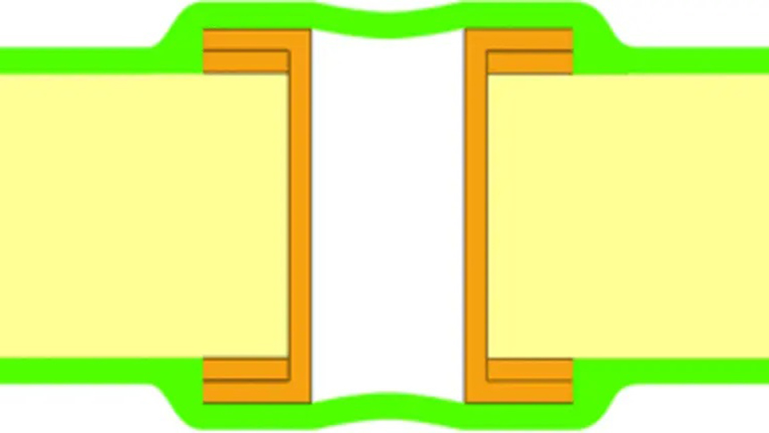
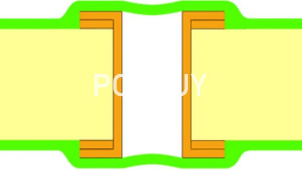
In modern PCB manufacturing, tenting vias PCB refers to the process of covering through-holes (vias) with solder mask or dry film in order to protect the copper surface from oxidation, prevent solder bridging, and improve electrical insulation. This technique is widely applied in HDI designs, BGA layouts, and other high-density circuit boards where reliability and precision are essential.
At PCBBUY, we specialize in advanced via protection technologies including tenting vias, plugged vias, and via-in-pad solutions. Our goal is to ensure that every circuit board meets the highest standards of durability and functionality, while also offering cost-effective options for global customers.
Why Tenting Vias PCB Matters in PCB Manufacturing
The main advantages of tenting vias PCB include:
-
Oxidation Prevention: By covering exposed copper rings, tenting reduces oxidation and corrosion.
-
Solderability Control: Prevents solder from flowing into vias during reflow or wave soldering.
-
Improved Insulation: Creates an additional dielectric barrier between circuits.
-
Extended Reliability: Helps maintain long-term electrical stability, especially in compact, multilayer designs.
This method is especially valuable in BGA (Ball Grid Array) assemblies, where open vias can cause solder shorting or reliability issues.

Tenting Vias PCB Process at PCBBUY
At PCBBUY, we follow a strict workflow for tenting vias PCB to ensure consistency and reliability:
-
Design Review – All Gerber and drill files are carefully analyzed to determine which vias should be tented, plugged, or left open.
-
Solder Mask Application – Vias are covered with solder mask ink or dry film. Proper thickness and alignment are maintained to achieve full coverage.
-
Exposure and Development – The solder mask layer is exposed and developed under controlled conditions to ensure precision.
-
Thermal Curing – The boards undergo curing to achieve hardness and adhesion of the solder mask.
-
Inspection and Quality Control – AOI inspection and cross-section analysis verify the integrity of the tenting process.
Key Standard: In tenting vias PCB, the industry standard is that the through-hole should not retain tin in the soldering furnace. A certain level of hole redness is considered a normal process phenomenon.

Tenting Vias PCB vs. Plugged Vias
Different via protection techniques are applied depending on application needs.
|
Via Protection Method |
Process |
Advantages |
Limitations |
|
Tenting Vias PCB |
Vias covered by solder mask |
Cost-effective, prevents oxidation and solder bridging |
Limited protection for large or high-reliability vias |
|
Plugged Vias |
Vias filled with epoxy or solder mask |
Stronger barrier, flat surface, suitable for BGA pads |
More costly, requires stricter process control |
|
Via-in-Pad (Copper Capped) |
Electroplated copper filling |
Excellent electrical and thermal conductivity |
Complex process, higher cost |
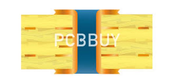
Plugged Vias Standard: According to industry practices, the standard of plugged vias is based on the impermeability to light (no white light visible through the via). For vias larger than 0.45mm, partial filling is possible, but no cavity should remain. A fully plugged via shows no light penetration.

Quality Assurance for Tenting Vias PCB at PCBBUY
To guarantee the highest quality, PCBBUY applies multiple inspection methods:
-
AOI (Automated Optical Inspection) – Ensures that vias are fully covered with solder mask.
-
Cross-section Analysis – Confirms no cavities remain in plugged vias.
-
Thermal and Humidity Testing – Validates long-term reliability under extreme conditions.
-
Compliance with IPC Standards – All tenting vias PCB and plugged vias processes follow IPC-A-600 and IPC-6012 requirements.
Applications of Tenting Vias PCB
Tenting vias PCB is widely used across industries:
-
Smartphones and Tablets – Compact HDI boards with BGA layouts.
-
Automotive Electronics – Enhanced reliability for harsh environments.
-
Medical Devices – Precision PCBs requiring strict insulation.
-
Industrial Control Systems – Stable performance under heavy-duty operations.

Why Choose PCBBUY for Tenting Vias PCB?
PCBBUY offers complete PCB solutions with advanced tenting vias PCB and plugged vias capabilities. Our advantages include:
-
State-of-the-art solder mask coating and exposure equipment.
-
Engineering expertise to optimize via designs based on customer requirements.
-
Flexible production from prototypes to high-volume orders.
-
Proven experience serving clients in Europe, North America, and Southeast Asia.
Conclusion
Tenting vias PCB is a cost-effective and widely used solution for protecting vias, preventing oxidation, and improving soldering performance. At PCBBUY, we combine advanced solder mask technology, strict process standards, and comprehensive inspection systems to ensure every PCB we manufacture delivers exceptional quality and reliability.
If you are looking for a reliable manufacturing partner for tenting vias PCB or other advanced PCB solutions, PCBBUY is ready to support your projects from design to mass production.
Industry Category


