Test Point PCB Design
By:PCBBUY 08/23/2021 09:47

The circuit boards we design also have some testing to go through; and, in their case, the testing will determine how well they have been manufactured. In order for this testing to happen, the board must be prepared with specific elements that a test probe can access. These elements are called test points and their inclusion on PCB designs is very important.
In this passage, we will focus on the topic and if you are curious about it, please check and read our content below for more information or FOR PCB QUOTE HERE.
Why to process test points on PCB?
To verify the integrity of the component assembly process, a completed printed circuit board will go through an automated test cycle. This is designed to find component pins that are not connected to the board with a good solder joint and will use a system of probes to contact the test points designed into the board. There are two different systems that are generally used for this testing:
In-circuit test (ICT)
This is a system that is designed to test all of the nets on the circuit board simultaneously. To do this, ICT employs the use of a test fixture that is loaded with probes to contact the test points on the board. The fixture will have one probe for each test point on the board, which enables the testing to be conducted very quickly. These test fixtures are usually configured to test the bottom of the board, but they can also test the top or both sides of the board at the same time.
Because the ICT fixture is designed to test each circuit together, it is the test method most likely to be used for production runs of a circuit board. Another advantage is that ICT can also conduct some functional testing of the board in addition to the manufacturing tests. The drawback, though, is that ICT fixtures take time to develop and are expensive to build. Alterations to existing fixtures for PCB design revisions can be costly as well.

Flying probe
This system differs from ICT in that it only uses between two and six probes to conduct all of the tests on the board. As the name would suggest, these probes fly around the board contacting each specific test point sequentially that they are programmed to test. Due to the more individualistic nature of the testing, the flying probe takes a lot longer to test a board than an ICT will. Flying probes also aren’t able to conduct any functional testing of the board due to the minimum amount of test points that are being probed at one time.
The advantage of the flying probe test, however, is that it is very fast and inexpensive to set up and run. Additionally, alterations to the test due to circuit board revisions are easy to incorporate. Flying probe systems can also test larger board sizes than ICT systems can.
What are the different types of test points of PCB?
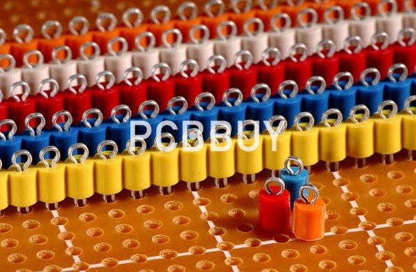
There are two main types of test points used on a printed circuit board. The first is an easily accessible point for a technician to access with hand-held testing equipment. To help with this, these points often have a post soldered into them for clipping on a test lead. These test points will be marked with a reference designator and usually the name of the net in silkscreen for easy reference, such as “GND.”
The other type of test point is used primarily for automated test equipment. The automated test points on a circuit board are thru-hole pins, vias, or small landing pads of metal that are designed to accommodate the probes of automated test systems. There are three main test systems that will use these test points on the board:

Bare board test: This is a test that is run after the circuit board has been fabricated to make sure that all of the nets in the board have electrical connectivity.
In-circuit test: ICT is run after the board has been assembled. The board is positioned on the ICT fixture which is filled with probes for each individual net. These fixtures usually test the bottom of the board, but they can also test the top or both sides together if needed.
Flying probe: Like ICT, this test is run after assembly on each net of the board by accessing the test points. Where it differs, however, is that the flying probe equipment uses two to six probes that move around to each test point instead of using stationary probes in a fixture like ICT does.
How to use test points of PCB?
Refresh Yourself on Test Points
There are two different types of testing that require a PCB test point: bench testing by a technician and automated testing during manufacturing. We will be talking about the latter here, and there are two types of automated tests that use test points: bare-board testing for fabrication and in-circuit testing (ICT) for assembly.
The bare-board testing is done prior to assembly and it is to make sure that you have good electrical connectivity between all the nodes. The ICT is a more functional test after assembly to make sure that the components are working as they should. In both cases, probes from a test fixture will come into contact with the test points on the circuit board in order to conduct the tests.

Assign a Test Point Manually
The general rule of test points on a printed circuit board is that each net needs to have a probeable point to test. These “test points” need to be known and cataloged in the Printed Circuit Board design system for reports to be generated that the manufacturer will use when testing the finished boards. To do this you will create test points on the board by flagging pads or vias as probeable points. Altium Designer has capabilities to do this both manually and automatically.
Test Point Design Rules
You can set up design rules in Altium Designer for governing the size, spacing, and clearance requirements of the pads and vias to be used as PCB test points. These setups are in the “PCB Design Rules and Constraints” menu, which can be accessed from the Design > Rules pulldown menu.
Industry Category


