The Top 10 Popular PCB Abbreviation List to Learn PCB Basic Knowledge
By:PCBBUY 11/01/2021 09:58

Are you a beginner of PCB industry? Do you know the basics of PCB knowledge? If you are interested in PCB basic knowledge, you can check and read the content below In this passage for more professional information.
What is PCB?
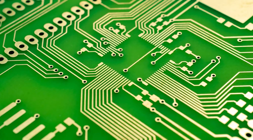
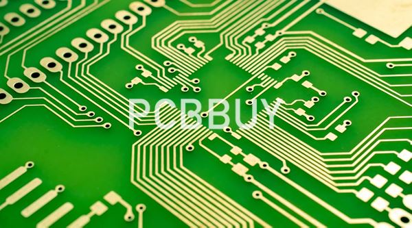
PCB is the acronym of Printed Circuit Board, a mechanical base that contains tracks and footprints reflecting the schematic of the design. Modern PCBs are typically made of a non-conductive substrate that is over layed by copper layers.

The copper areas on the PCB are etched to form pads, vias, polygons, and traces that connect the respective components. Designators and silk screens are printed on to aid the assembly process. A layer of solder mask is applied to protect copper traces from corrosion and short circuit, particularly during the soldering process.
What is the history of PCB?
The modern world that we know today won’t exist without printed circuit boards because it is the backbone of the electronics which holds all the components mechanically and conducts electrically. A PCB can hold hundreds or even thousands of components and makes sure the components and its connections stay unaltered even when we apply mechanical shocks and this is the primary function of a PCB.
The idea of PCBs or something very close to that can be tracked back around 1900s and several famous inventors were also got involved in it including Edison and several patents has been granted to several inventors for their method of fabricating PCBs.
Despite the idea of PCB existed as early as 1900s, till 1950s PCBs did not conquer the consumer market, but still people had electrical appliances like televisions and radios at their home. The home appliances were manufactured without PCBs looked like this:
What are the top 10 PCB abbreviations?
1. FR4 – Flame Retardant 4
This is a common insulation material for making PCBs. It is made of woven glass fibres (fiberglass), which are epoxies together. FR4 glass epoxy is a common and versatile high-pressure thermoses plastic laminate grade with high strength to weight ratios.
2. Multilayer PCB
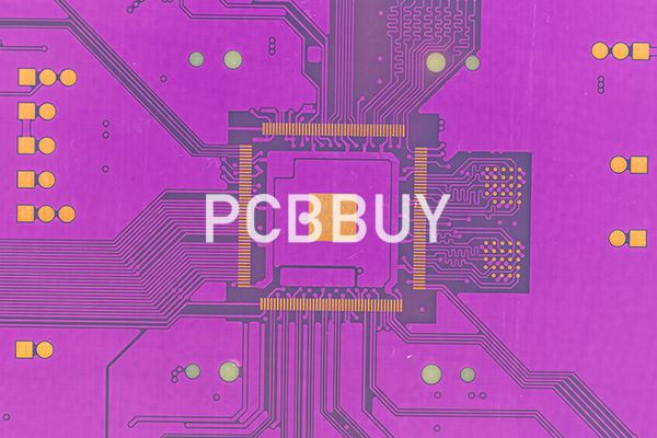
A circuit board with more than two conductive copper layers. They look like several layers of double-sided PCBs, laminated and glued together with layers of heat-protective insulation between them. The construction of a multilayer PCB is designed so that two layers are located on the surface sides of the board to connect to the environment.
3. PCBA – Printed Circuit Board Assembly
A process linking the electronic parts with the wirings of a bare circuit board. The conductive pathways etched in the laminated PCB copper layers are used in a non-conductive substrate to create the assembly. Connecting components to a bare board is the concluding activity towards obtaining a fully operational electronic gadget.

4. Silkscreen
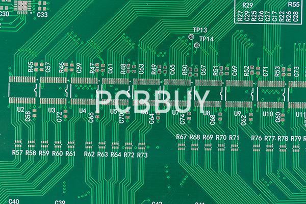
A layer of epoxy ink applied to a circuit board that bears components labels and positions. The labels guide engineers throughout the assembling process. Normally, silkscreens are white, distinguishing the labels from the solder mask.
5. AOI – Automated Optical Inspection
This is an automatic visual inspection method used to test defects in printed circuit board assembly (PCBA). AOI autonomously examines the PCBA process for catastrophic and quality failures.
6. BOM – Bill of Materials
A comprehensive list of the raw materials, assemblies, subassemblies, components, and quantities of each required in PCB manufacturing. A BOM is normally written in a hierarchical format, with the highest level describing the end product and the bottom level highlighting individual components and materials.
7. HASL – Hot Air Solder Leveling
Surfaces finish process where a thin layer of solder is applied as a protective cover on the exposed copper parts. HASL is the cheapest surface treatment and is the common surface finish in most PCB fabrications. Though some systems can deposit a fairly uniform coating, this method leaves a rough surface compared to other methods, like ENIG.

8. Laminate
A combination of various materials via heating, adhesive and welding processes forms a new material with several layers. The end product (laminate) is stronger and more stable than the individual materials used to create it.
9. Substrate
This is basically a PCB base material – the main material for printed circuit board fabrication. A substrate can be flexible or rigid and can contain epoxy, metallic, or ceramic properties. The PCB application normally determines the type of substrate to use.
10. Dry Film Solder Mask
A film mask applied to a PCB to achieve a higher resolution mask with finer line designs. However, this method is a bit more expensive than other methods, like liquid solder mask.
Industry Category


