Thermal Management in PCB Design
By:PCBBUY 08/18/2021 17:18

To avoid failures or circuit malfunctions, designers should aim at producing PCBs that operate and remain within safe temperature limits. Most electronic components dissipate heat whenever a current flows through them. There are situations where adding heat sinks, cooling fans, or a combination of several mechanisms is inevitable.
Want to learn more professional knowledge about thermal management in PCB? Please check and read the content we provide below to get more information. Let’s go!
If you want to order PCB product, please check and custom your order online.
Why thermal management in PCB is necessary?
In high power density PCB, it is difficult to control heat generation. This occurs because there are many channels of traction power at the same time and many elements that depend on the current supply at the same time. High power density PCBS are not necessarily bad designs; Some applications require high power density to perform various functions. In these cases, the efficient use of space is critical, as any crosstalk may quickly cause a thermal peak.
Some high power density PCB requires large components, which increases the complexity of their thermal management. Large components naturally generate more heat, but they also reduce the available surface area on the PCB to dissipate heat. Keeping enough cooling area on a PCB is an important part of keeping it cool; Packing components together as tightly as possible to cover the board, even if they all meet IPC standards, can be harmful.
What are the techniques of thermal management in PCB?
PCB fabrication requires both heat and pressure in order to laminate the layers together, while the soldering process will heat the board up during assembly. Wave soldering will run the exposed components leads on the bottom side of the board through a molten wave of solder, and solder reflow requires the entire board to be baked in an oven. Here are some of the thermal problems that are associated with circuit board manufacturing:
Bow and twist: If the metal coverage throughout the different layers of the board is not consistent, it can cause the board to bow or twist during fabrication. For instance, if the first three layers of a six-layer board have a higher percentage of metal than the bottom 3 layers, the board will be out of balance. This imbalance can result in the board warping as the high heat and pressure are applied during fabrication.
Bad solder joints: These often happen because the metal around the pin to be soldered behaves as a heat sink and robs heat from the connection during wave solder. As a result, the solder doesn’t melt correctly, leaving a cold and unreliable solder joint. The solution in cases like this is to use a thermal relief pad to concentrate the heat on the solder joint.
A thermal relief pad from a PCB design CAD system A thermal relief pad like this will help focus the heat on the pin to create a better solder joint
Tombstoning: This is a condition where a thermal imbalance between the two pins of a small surface mount component causes the part to stand up vertically during solder reflow, just like a tombstone. The thermal imbalance occurs when one of the pins is connected to a large area of metal, which acts as a heat sink. This allows the solder on the other pin to melt faster pulling the part up with it. To prevent this, PCB designers should use thermal relief type connections when connecting pins to large areas of metal.
What are the considerations of thermal management in PCB?
As a carrier of the components, the printed circuit board is the main component for achieving coherent thermal management. Inadequate optimization must be compensated later by possible cost-increasing measures.
In advance, the following basic considerations should be made:
1. Which amount of heat (power loss) must be removed?
2. What are the dimensions and performance data of the components?
3. Where are the heat sources (such as LEDs) on the PCB?
4. What are available space and mounting peripherals?
5. What are application temperatures and ambient temperatures?
6. What mechanisms are used to cool the system?
7. How should heat be conducted to the heat sinks?
8. Are there certain reliability requirements?
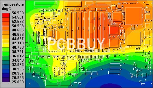
How to identify thermal problems of PCB?
Designers can use a variety of techniques to identify potential problems. Popular methods include the use of thermal analysis tools, visual inspection, and infrared cameras.
Conduct thermal analysis
Thermal analysis can be performed to determine the performance of components and PCB at different temperatures and conditions. The analysis results provide designers with ideas of heat generation and transfer in circuit. Designers can then use the analysis and simulations to come up with techniques to help them better manage heat.
Visually inspect the board without power
Visual inspection is an easy way to find signs of overheating, burnt or partly damaged components, dry joints, arcing, etc. Some of the visible signs include bulging components, burnt components, and discolored spots on the PCB. In addition to the visual analysis, a smell from the board can also point to heating issues.
Use infrared cameras
Test engineers can use IR cameras to evaluate powered prototype boards for heat problems and identify issues invisible to the naked eye. In addition to showing areas where there is excess heat, the cameras can sometimes identify counterfeit or defective parts whose thermal signatures differ from those of genuine components. Thermal imaging cameras can also detect the location where the tracks have insufficient solder, hence higher resistance and more heat dissipation.
Industry Category


