Top 5 Effective Suggestions for PCB Design Guidelines for Beginners
By:PCBBUY 11/17/2021 09:33

Generally, a layout denotes the way the parts of a specific item are laid out or arranged. In the same vein, a PCBlayout is a broad term indicating several processes required in designing a PCB. It involves making traces, mounting holes cutouts, labeling, and specifying component locations, among others.
And if you are a beginner of PCB design, we will provide you all the information of the guidelines. If you are interested in the PCB design guidelines, please check and read the content below in this passage for professional knowledge.
If you want to order PCB product, please check and custom your order online.
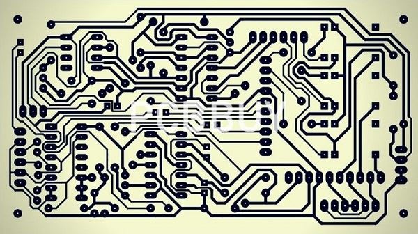
1. What are the common technologies of PCB design?
PCB designers must be able to develop excellent layout designs for the proper functionality of components that use printed circuit boards. Lately, there is a huge demand for PCBs with minimal footprints. Printed circuit board designers are therefore required to employ the use of smaller components that reduce footprint significantly. Generally, components that find use here are very close to each other.
If you happen to select an incompetent layout technique, then the connection may go wrong and affect the functionality of where it will find useful. Sadly, most printed circuit board manufacturers find it hard coming up with the best layout. The greatest challenge faced is when handling the device with higher pin counts and a smaller pitch. If the layout is wrong or incompetent, rest assured that the board will fail to function as desired.
To ensure the desired functionality, it is very important to select the best layout technique available in the market. If you are in the market for the best PCB designer, look no further after comparing several companies. They must understand nearly everything to do with the board layout and ready to assist you all the way.
2. How to choose the proper software?
One of the best things you can do to improve the quality of your PCB design is to use quality software for the creation. Of course, some might worry that software will be expensive or difficult to use. While this is certainly a potential problem with some pieces of software, it doesn’t have to be.
Advanced Circuits offers PCB Artist, a robust piece of software that can provide you with the guidance and tools you need for your PCB design regardless of how simple or complex it might be. It offers more than is found with most other pieces of software on the market that provide similar features. One of the best features of the software is the price. It is entirely free, so you will not have to worry about paying anything when you are getting started. Whether you are a hobbyist or working for a company, you will appreciate this benefit.
While the software will have a learning curve, like any piece of software, it tends to be easy to use. Those who have any experience with PCB design should not have a problem getting started with the intuitive software.
3. How to choose the right components?
As a board designer, you should thoroughly study the BOM and examine the parts that go into the design. When there is sufficient space on the board, you may opt for larger components for resistors and capacitors. It is beneficial to use a 0603 or 0805 size capacitor/resistor instead of a 0402/0201. Select the smaller package version of the component if you have spacing issues. Moreover, choose your appropriate component and package based on the required current, voltage, and frequency.
Smaller components are manufactured by various vendors. It allows designers to choose alternate parts without modifying the schematic or layout, providing a timely solution for components that are not in stock. Furthermore, it is crucial to decide the appropriate size of the package during the PCB design phase. It is recommended to choose smaller packages only when necessary; otherwise, choose larger packages. Using too many small component packages can create issues during circuit board assembly, which leads to difficulties during cleaning and reworking.
4. How to avoid the common issues of PCB layout?
Errors in landing patterns
PCB design software packages provide libraries of electronic components. These libraries include the schematic symbol and PCB landing pattern for each component. You won’t usually have problems if you stick to these components in your design.
However, if you use components outside of these libraries then you must manually draw the schematic symbol and the PCB landing pattern. It’s easy to make mistakes especially on the landing pattern. For instance, if the pad to pad spacing is off by as little as a fraction of a millimeter, the pins won’t align properly making soldering difficult or impossible.
5. How to process the right trace width in PCB layout?
The trace geometry (thickness and width) is of fundamental importance to ensure the correct operation of the circuit in all environmental and load conditions. The traces of a PCB are used to carry electrical signals and, therefore, must have a width compatible with the current passing through them. The designer must determine the minimum width of each trace in order to avoid dangerous overheating of the board; this parameter directly affects the routing process, as it reduces the space available on the PCB. The minimum width must therefore be determined before placing the traces, using one of the several calculator tools, also available online. By entering thickness, current and maximum acceptable temperature rise, these tools return the minimum trace width.
PCB trace thickness is measured in ounces of copper, corresponding to the thickness that would be obtained by uniformly distributing an ounce of copper over an area of one square foot. This thickness is 1.4 thousandths of an inch. Standard PCBs use 1- or 2-ounce thicknesses of copper, but for high current applications this can be as high as 6 ounces. If the available space is not an issue, the advice is to use traces with a width greater than the minimum, thus improving the thermal management and reliability of the board. Also keep in mind that the traces on the outer layers achieve a better heat exchange and, therefore, may have a smaller width.
Industry Category


