Top 5 Effective Tips of BGA PCB Layout Guidelines for PCB Manufacturing
By:PCBBUY 11/13/2021 10:13

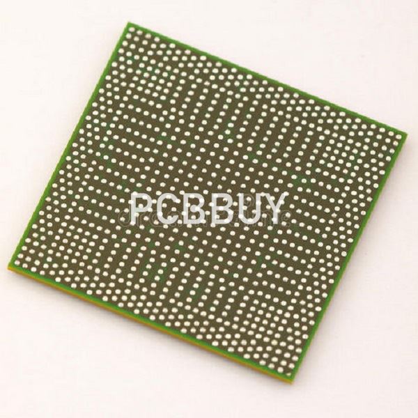
There are many types of BGA packaging; the general shape structure is square or rectangular. According to the arrangement mode of solder ball welding, it can be divided into peripheral type, staggered type and full array type BGA. According to the different substrates, it will divided into several types
Are you going to learn more about details of BGA PCB layout? If you are searching for BGA PCB layout, you can check and read the content below for more knowledge in this passage.
1. What are the rules of BGA PCB layout?
Currently, the standard for housing a variety of advanced and multifaceted semiconductor devices like FPGAs and microprocessors is done through Ball Grid Array (BGA) device packaging, using the BGA component. BGA packages for embedded design has evolved significantly over the years, to keep up with the technological progression of chip manufacturers. This particular type of packaging can be broken down into standard BGAs and micro BGAs. With today’s electronics technology, the demand for I/O availability poses a number of challenges, even for experienced PCB designers, due to multiple exit routes. What are some strategies we can use to successfully overcome these BGA PCB design challenges?
2. How to avoid BGA PCB defects?
During the process from lead manufacturing to lead-free manufacturing, reflow soldering and wave soldering temperature has to rise up due to SMT (surface mount technology) assembly requirement. Some people simply believe it OK that substrate material with high Tg (glass transition temperature) is selected for PCB board. They just think that it's essential to manage and control Z-axis expansion.
The primary aim is to stop delamination from taking place of thick circuit boards and 14-layer or more PCBs and to stop cracks from occurring to PTH (plated through hole) because a large extent of Z-axis expansion of PCB tends to lead PTH hole wall to break during reflow or wave soldering. Nevertheless, Tg fails to defeat cracks generated during lead free process unless Td (temperature of de-composition) is considered to totally solve PCB cracks issue. Three levels of Td are regulated in IPC concerning PCB substrate material: 310°C, 325°C and 340°C.
3. How to process the BGA PCB layout control?
· During stencil design phase, four corners and each side of BGA component should be 1mil to 2mil larger than those of pad. Stencil opening size should be designed based on specs of BGA components including pitch, soldering balls on BGA and ingredient of soldering balls.
· During the process of printing, support pin shouldn't be against BGA to stop fake soldering and pillow effect from taking place due to contamination of BGA pad. Furthermore, especially much attention has to be paid to printing scraper pressure and printing quality control.
· Wafer positions of pickup BGA, component thickness setting and pressure amount of pickup should be emphasized during mounting stage.
· There are more opportunities for cracks during IR reflow and special attention has to be paid:

4. What are the challenges of BGA PCB layout?
BGA routing presents unique challenges that must be considered as you design your PCB. The most significant of these involve ensuring the signal integrity, manufacturability and reliability of your board.
Signal Integrity
A key signal integrity issue is impedance control, which affects transmission and reflections. The impedance can be controlled by matching trace widths between forward and return lines, using the appropriate dielectric thickness and installing a reference plane between signal layers. Installing reference or ground planes between adjacent signal traces is also effective in minimizing crosstalk. When the signals are on the same layer, maintaining the spacing between traces is key.
Manufacturability
In addition to determining the number of layers (signal and reference) to optimize signal integrity, you need to consider the manufacturability of the BGA routing scheme. There are specific restrictions and guidelines depending on how the BGA connections are routed with each other and externally. The number of layers, pitch angles, via sizes, type of hole drilling and other concerns are limited by the capabilities of the manufacturer.
Reliability
The reliability of your PCB depends on board construction quality and synchronization of your design with the capabilities of your manufacturer by employing good DFM practices. Not synchronizing or pushing the limits too far can result in boards that don’t function as designed or may fail at some point once deployed in the field. Copper weight, solder mask thickness, copper grain structure and ionic contamination are material issues that cause failure in the field. Trace routing, including via choices, may also affect operation, leading to significant costs for recalls and replacements.
5. What are the advantages of BGA PCB layout?
With PCB BGA, you will get the following advantages:

BGA package eliminates the issue of developing small packages for ICs with lots of pins. Traditionally, dual-in-line and pin grid arrays surface-mount boxes had very little space between the pins. They provided a considerable disadvantage for the soldering process with more pins. However, you will not need to worry about accidentally soldering together two pins with BGA packages.
Again, when compared with packages with legs, The BGA package has a lower thermal resistance when placed on the PCB QUOTE. That permits the heat that IC produces in the box to conduct through the PCB efficiently. Of course, it will save your chip from overheating.
Do you know which property causes unwanted signals distortion in high-speed electronic circuits? The unwanted inductance in an electrical conductor is responsible for this phenomenon. However, BGAs have very little distance between PCB and the package, leading to lower lead inductance. Thus, you will get top-class electrical performance with pinned devices.
Industry Category


