Top 5 Essential Factors for HDMI PCB Layout Guidelines
By:PCBBUY 12/09/2021 09:11

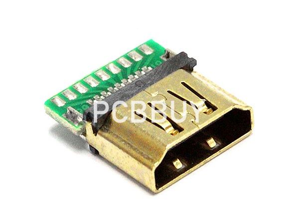
In printed board circuits, HDMI can be used for sending high-rated signals from one port to another. Normally HDMI traces on boards are very short, directly from the connector to the receiver/transmitter. Many times we get the question of how long can I make HDMI traces. The HDMI specification does not define maximum length, only expected impedance. As long as you follow the layout rules above you should be able to run HDMI traces over 20-30cm easily.
Analog Devices HDMI components are designed so routing is a straight shot from the device pin to the connector pin. However sometimes you need to change layers the HDMI routing is done on, often changing the reference ground plane in the process. If you are going to learn more about HDMI PCB layout, please check and read the content below for more information.
1. What are the applications of HDMI PCB?
HDMIs are serving in DVD, Media players, Play stations, Xbox, TV, and other digital devices for domestic’s purposes. In AV commercial market, laptops and PCs are using HDMI PCB rather than simply connecting cables. So in the corporate market, the value of these PCBs is increasing day by day. From education, transformation, presentation to engaging, retail displaying, and transmitting high-quality content, HDMI PCB is everywhere. HDMI PCB also solves the problem of analog that requires separate audio and video devices. Moreover, a single HDMI PCB can transmit enhanced, high quality, and standard video signals by offering up to 6 channels for transferring digital data.
2. What are the rules of HDMI PCB layout?
Layout is the key. The following is a general set of rules that has become part of my layout specification for boards. They are a bit tighter then the math above indicates but are easily met during layout. These rules can be added directly as constraints to your schematic or as part of the layout specification document.
· Each HDMI channel is comprised of 4 TMDS pairs.
· Each HDMI channel set shall be routed primarily on the top or bottom layer as a group or alternately routed as a group on internal layers.
· TMDS pairs in each HDMI channel shall have matching lengths of ± 3mm.
· HDMI channel sets shall be separated from other HDMI channel sets by a minimum of 7.8 mm.
· HDMI channel sets shall be referenced to an adjacent solid ground plane.
· If a HDMI channel set must transition to another reference ground plane then ground plane to ground plane vias must be added adjacent to the channel transition vias.
3. What are the different traces of HDMI PCB layout?
HDMI uses transition minimized differential signaling (TMDS) for transmitting high-speed serial data. Differential signaling offers significant benefits over single-ended signaling.
In single-ended systems, current flows from the source to the load through one conductor and returns via a ground plane or wire. The transversal electromagnetic wave (TEM), created by the current flow, can freely radiate to the outside environment causing severe electromagnetic interference (EMI) (Figure 3 ). Also noise from external sources induced into the conductor is unavoidably amplified by the receiver, thus compromising signal integrity.

4. What are the discontinuities of HDMI PCB layout?
Discontinuities are locations in the signal path where the differential trace impedance deviates from its specified value (of 100 15 percent for HDMI), and assumes either higher or lower impedance values. Discontinuities cause signal reflections due to impedance mismatch compromising signal integrity. These are primarily the result of changes in the effective trace width or in the line-to-line spacing caused either by unavoidable transitions in the trace geometries along the signal path, or by poor routing of the signal traces.
Potential locations for discontinuities are:
· Where the solder pads of the HDMI connector meet the signal traces
· Where signal traces meet vias, component pads of resistors, or IC-pins
· 90o bends in signal traces
· Where a signal pair is split to route around an object
5. What is the importance of HDMI PCB layout?
You may have heard about HDMI when it comes to tech-related electronic devices but do you exactly know the meaning of it? Well, here we have tried to explain it readily. HDMI stands for high definition multimedia interface. HDMI was introduced by many companies such as Sony, Toshiba, etc. the reason was, and a single HDMI was replacing three different types of audio and video connectors in digital devices. These are the highly suggested interfaces that are used to send both videos and audio with HD signals.
In printed board circuits, HDMI can be used for sending high-rated signals from one port to another. All the electronic devices that are suing PCBs for technical purposes such as laptops, mobile phones, and many medical types of equipment are also using HDMIs in their construction for better functionality. Both commercial and domestic sectors are relying on HDMIs for connecting purposes mainly. HDMI connectors are the best possible choice for transferring data such as videos and audio. We will also read about HDMI connectors in this article.
Industry Category


