Top 5 Essential Factors of PCB Panelization Design Guidelines in PCB Layout
By:PCBBUY 11/12/2021 09:22

Multiple panelization methods exist, each with its own drawbacks and benefits. The design of the boards on the panel and the panel itself will often play a large role in which panelization method best suits the application. The most notable of these factors include:
If you are curious about PCB panelization knowledge, you can check and read the content below in this passage for more information.
1. PCB panelization improves work efficiency
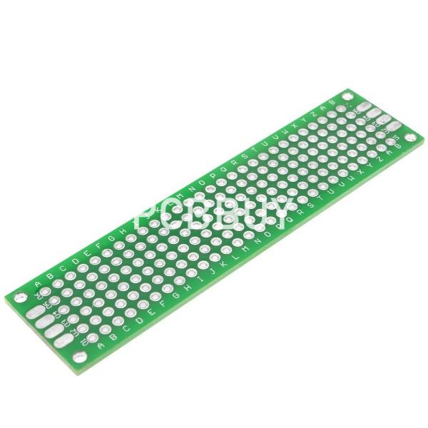
As a way of improving the productivity of the PCB manufacturing process, it is common practice to mount several copies of smaller printed circuit boards in a manufacturing panel. It is an effective method of fabricating and assembling the boards instead of building them one by one. The panel must contain the same materials and layer stack-up configuration as the printed board.
It is also essential to choose the size of the panel, whether small or large, that best fits your printed circuit board's needs and the various manufacturing and assembly processes. The more boards you can fit into a PCB panel, the more efficient the manufacturing process will become. It will also reduce the number of panel space that will go to waste.
During panelization, PCB panel designers must use all the arrangement options when placing the PCB designs to optimize the panel space and improve manufacturing efficiency.
2. How to process the PCB panelization design?
One of the biggest and costliest mistakes designers make is to leave essential PCB guidelines as an afterthought. Instead, they devote all their time to component selection and circuit design. Why is this a problem? Well, if you do not provide sufficient time and effort to the basics of PCB layout, you are likely to end up with a circuit design that performs poorly, both from the digital domain to the physical reality. The final design becomes problematic for the PCB manufacturer to fabricate.

So how does the designer create a design that is both realistic on paper and in physical form? The first thing you need to know is there is not such a thing as a standard PCB. Every circuit board performs a unique function in the particular product you intend it for.
As a board designer, you will need to use a computer-aided design system with special design software to layout your circuit pattern on the board. Often, the space between two electrical conducting paths is 0.04 inches or less. Using the design software, you will also need to layout the holes’ location for contact points and components. All this information is essential for the computer-controlled drilling machine during the manufacturing process.
As soon as the circuit pattern is complete, your computer-aided system prints out a negative image, also known as a mask, on a clear plastic sheet. This mask is the exact size of the circuit board. All areas that will not be part of the circuit pattern appear in black while the circuit pattern is clear.
3. What are the main factors of PCB panelization design?
· Panel size: There are different sizes of panels that are used by manufacturers, with some that are more common than others. The size of your circuit board will have a big influence on what panel size is ultimately chosen due to how it will be laid out in the panel. It is a good idea to work ahead with your PCB contract manufacturer in case the board size can be altered to fit more instances into the panel.
· Layer stackup: One advantage of a panel is that multiple circuit boards can be laid out in it, but the layer stackup has to be uniform for all boards. If you are planning on panelizing multiple boards, make sure that they have identical layer stackups.
· Panel structure: The instances of boards will need specific clearances to each other and to the edge of the panel, and will usually include alignment holes and other features. Once again, working ahead with your CM will help you in the end to have a finished board size that can be easily panelized.
4. What are the considerations of PCB panelization design for designers?
While PCB designers can do their own panels, it is generally advisable for the contract manufacturer to do this work. Ordinarily, the PCB CM is already working with the fabricator on the build and designing the panel based on the size, shape, assembly criteria, and expected volume of production. The CM also has a lot of experience in panelizing boards and understands the different requirements needed such as location, the spacing of breakouts, and other panel features.

5. How to make standard PCB panelization design?
In designing of a panel 2 main physical requirement must be kept in mind, Mechanical Stability and Strength: it is to be considered that the pcb must be submitted to several handling and other processes ( and some of them are hi themperature processes) so the panel should be constructed to resist at all these processes (both during PCB production and the final PCB assembly): if it break probably none pcbs could be used.
Obviously that the Panel Manufacturability and Ease of Board’s Assembling are also important panel characteristics and requirements. Panel layouts that are hard to produce (or impossible to do) or which could create extra problems during board’s assembly, could be rejected during CAD/CAM operation.
Mechanical technology that permit pcb separation after assembling processes could be break-routing (with breaking taps), or V-cut (scoring) or combinations of them.
Industry Category


