Top 5 PCB Manufacturing Challenges with PCB Prototyping Fundamentals
By:PCBBUY 09/23/2021 09:06
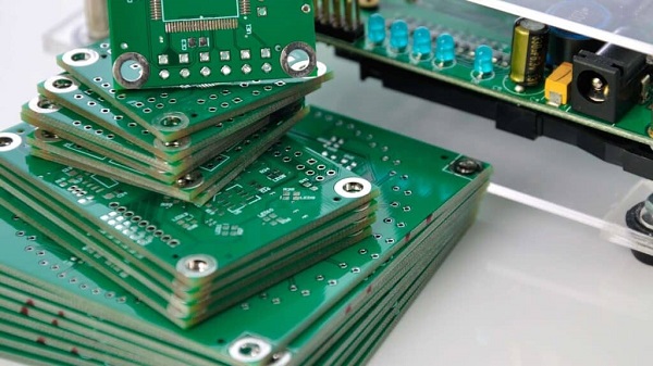
PCBs are thin plates of fiberglass, composite epoxy, or other laminate material inscribed ("printed) with conductive pathways that make it possible to connect components like transistors, resistors, and integrated circuits, so that data can be collected and distributed and functional networks can be established.
In this passage, we will provide you all the details about PCB manufacturing challenges. If you are curious about the PCB manufacturing process, please check and read the content for more professional knowledge.

What are the 5 common PCB manufacturing challenges?
Electronics and PCB manufacturing is presently facing several challenges together with opportunities. Along with the need to control costs, the PCB manufacturing services will have to focus on finding ways of capitalizing on current trends. This may include integrating technologies outside their primary areas of expertise, while meeting demands from customers for highly efficient manufacturing processes that are also eco-friendly. The biggest trends and challenges in the electronics manufacturing industries are likely to be:
1. Manufacturing is different from designing
The design of your PCB might look good on paper or a computer screen - but it can be an entirely different story when it comes to manufacturing it.
For example, there may not be sufficient tolerances between tracks on the board, which later on in the process could result in the circuit shorting out. Or perhaps the design includes a number of components positioned closely together, each with a different thermal mass. Achieving a quality solder joint on each of these components without heat damaging the rest of the circuit board requires expert process engineering skills.
If you are manufacturing a double-sided PCB, there are other factors to consider. Adopting this approach can allow you to fit more components into a limited space or to keep down costs. However, you will need to ensure that, where possible, your largest components are all placed on one side of the board and that this side is passed through the oven second. Otherwise, you risk these components falling off the board. You can use glue to hold down particularly difficult parts, but this requires additional manual work.
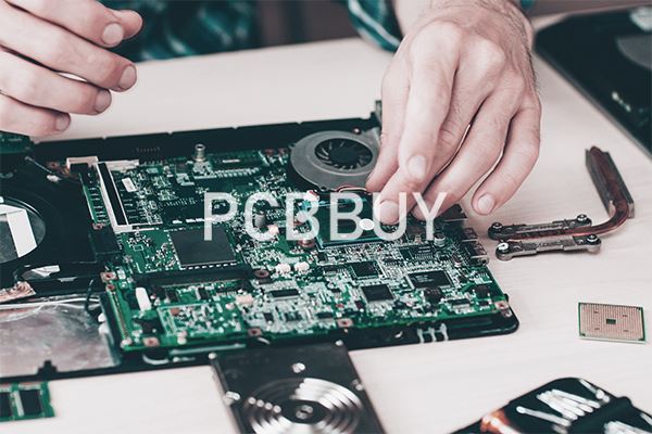
2. Insure the multilayer PCB stackup
Multilayer printed circuit boards are those boards that contain more than a single layer counts, hence the need for stack-up. Stack-up is the arrangement of insulating and copper layers to make a printed circuit board before the PCB layout design.
When it comes to the manufacture of multilayer printed circuit boards, challenges come in when it comes to pressing the insulating and copper layers together. A majority of multilayer printed circuit board manufacturers tend to encounter difficulties when it comes to pressing multilayer printed circuit board components together.
To ensure that the stacking process of multilayer printed circuit boards goes well, manufacturers need to ensure that they use the best machines suitable for the job in addition to using the best laminate materials.
3. Process the PCB manufacturing effectively
Injecting simulation into the PCB development process allows design engineers to identify potential manufacturing and assembly issues early in the R&D phase, before they reach downstream validation and physical testing stages. SDfM provides powerful tools to quickly and accurately recognize common PCB defects that would otherwise require extensive manual review or failed lab or field tests to uncover. Verification checks are a necessary step to reduce manufacturing cost and delivery time. However, PCB verification tools alone only go so far to improve production efficiency.
4. Pay attention high density interconnect
High density interconnect (HDI) was developed in response to the demand for smaller and smaller products with greater capability, especially in terms of routing traces. This capability that allows for fewer layers in the PCB stackup and promotes high-speed signal transmission. HDI manufacturing faces challenges with fabricating traces such that a greater number of traces may be routed within a smaller area, which introduces issues like noise and interference. Extensions of this concept, every layer interconnect (ELIC) and any layer interconnect (ALIC) should also see continued growth over the coming years.
5. Mention the components placement
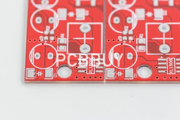
Component-to-component placement: As the circuit board is going through the wave solder, components that are too close to each other or rotated incorrectly can cause problems. For example, if taller components precede shorter components into the wave, it can result in a shadowing effect, which reduces the strength of their solder joints. Chip components rotated perpendicular to each other can result in the same issue.
Conclusion
PCB prototypes are slowly becoming pervasive in our daily lives, and this popularity will surely continue in the future. We can all agree that the increase in adoption results from increased consumer demand for smart and functional products. It is what you can observe in almost every industry; aerospace, medical devices, health, retail, and even the military.
Industry Category


