Top 5 Primary Aspects of Heavy Copper PCB Design during Manufacturing Process
By:PCBBUY 11/06/2021 10:06

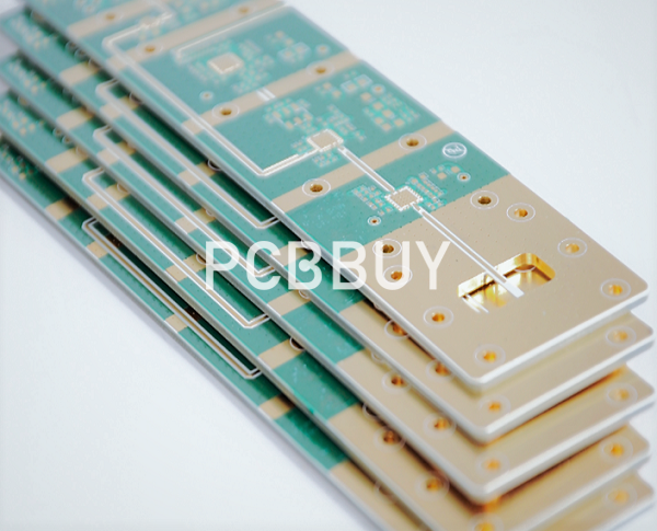
Heavy copper PCB is also known as thick copper PCB, in which there are 3 ounces (oz) of copper or more on the internal and external layers of a printed circuit board. The circuit board with a copper thickness of more than 4 oz per square foot (ft2) is also categorized as a heavy copper PCB. Extreme copper means 20 oz per ft2 to 200 oz per ft2.
If you are going to learn more about heavy copper PCB, please check and read the content below for more professional knowledge.
1. What is the structure of heavy copper PCB?
· Increased endurance to thermal strains.
· Increased current carrying capacity.
· Increased mechanical strength at connector sites and in PTH holes.
· Use of exotic materials to their full potential (i.e., high temperature) without circuit failure.
· Reduced product size by incorporating multiple copper weights on the same layer of circuitry (see Figure 1).
· Heavy copper plated vias carry higher current through the board and help to transfer heat to an external heatsink.
· On-board heatsinks directly plated onto the board surface using up to 120-oz copper planes.
· On-board high-power-density planar transformers
2. What are the military applications of heavy copper PCB?
· Weapons Control Systems
· Power Supplies for Radar Systems
· Primary and Secondary Windings of High Power Planar Transformers
· Power Distribution Panels
· Battery Charger and Monitoring Systems
Power electronics products using heavy copper circuitry have been in use for many years in the military and aerospace industry and are gaining momentum as a technology of choice in industrial applications. It's believed that market requirements will extend the application of this type of product in the near future.
3. What does heavy copper PCB offer?
Heavy copper PCB has a lot to offer. It has got some unique features that make it an ideal option for high-end applications. Let’s discuss some of the benefits of this PCB;

· Great thermal distribution: Due to its copper-plated vias, this PCB offers high thermal resistance. Heavy copper PCB are used in applications that demand high speed and high frequency. You can also use this PCB at harsh temperatures.
· Mechanical strength: Heavy copper PCB feature great mechanical strength. When this PCB is used, it makes the electrical system durable and robust.
· Good conductor: Heavy copper circuit boards are a good conductor. They are utilized in the production of electronics due to this feature. They help to link various boards together. These boards can transfer current.
· Onboard heat sink: Heavy copper boards offer an onboard heat sink. With these boards, you can achieve effective heat sinks on mosaic surfaces.
· Great dissipation factor: Heavy copper PCB are ideal for large components with a high loss of power. These PCBs prevent overheating from occurring in electrical systems. They dissipate excess heat effectively.
Supports exotic material: Heavy copper helps to protect and enhance exotic material. Exotic materials are sometimes used for designing electronic components. An extreme temperature may need an exotic material. Heavy copper boards end circuit failures because they use an exotic material to its full capabilities.
4. What are the capabilities of heavy copper PCB?
Prototyping is common in heavy copper product, UL approvals, and timelines. Knowing more helps us to help you succeed. Is this going to be an ongoing project for years to come? We have several options for production to produced small to large volume, or, is it a small one-time buy?
Explore stocking programs, EAU cost savings, and Kanban. All options are available at Epec.
· Maximum Number of Layers = 20
· Laminate - FR-4 (All Tg Ranges), Teflon, Ceramic
· Finished Thickness = 0.020" - 0.275"
· Green, Blue, Red, Black, Clear and White Solder Masks & Legend Inks
· Minimum Soldermask Clearance - 6 mils
· Minimum Solder Dam Width - 5.5 mils
· Hot Air Solder Leveling (HASL)
· Immersion Gold (ENIG) & Immersion Silver
· Blind & Buried Vias
· Minimum Drill Bit Hole Size = 0.012"
· Minimum Holes Size - 0.008" +0.005"/-0.008"
· Maximum Hole Aspect Ratio = 10:1
· Maximum Copper Weight = 6 oz. (UL Approved)
· Controlled Impedance +/- 10%
· Minimum Silkscreen Line Width - 8 mils
5. How to process the heavy copper PCB?
Heavy copper boards are fabricated using plating and etching techniques. The goal is to add copper thickness to via sidewalls and plated holes. Plated holes can weaken if a board is subjected to multiple cycles while in production, and the addition of heavy copper can strengthen these holes. Boards structured with heavy copper will allow for high current/power and control circuits on one board.

PCB manufacturers will check with customers and find out what their requirements are, and match the heavy copper fabrication process to specific needs. It will be important to know for example, the component type, layer count, and material requirements. The PCB manufacturer can quote the customer and present the pros and cons of using heavy copper. Advances in technology have created a process that utilizes both plating and edging.
Industry Category


