Top 6 Factors of PCB Board Dimension Tolerance to Ensure Product Quality
By:PCBBUY 11/02/2021 09:38

The story behind the standard PCB thickness is an interesting one that stretches back to the commercialization of integrated circuits. When electronic devices were transitioning away from discrete components and integrated circuits were being highly commercialized, PCBs were typically laid out by using a sheet of plywood as a breadboard.
Are you going to learn the knowledge of PCB board dimension? If you are interested in PCB board dimension, please check and read the content below for more professional information.

1. What is the standard of PCB board dimension?
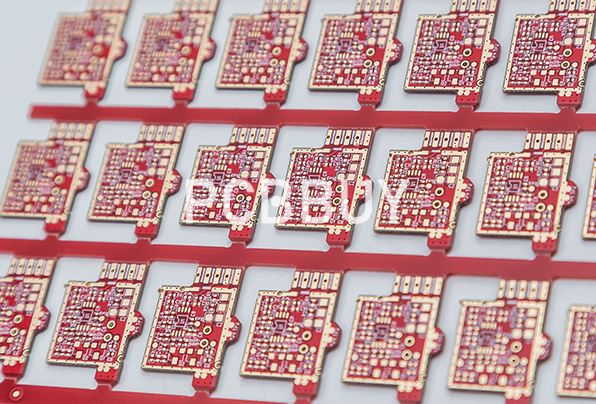
The panel size will limit the number of boards that can be reliably produced per panel. This means standard PCB panel sizes should be considered when floorplanning your board to maximize your yield per panel. Something as simple as rotating your boards or slightly modifying the board dimensions can help you produce a few extra boards per panel and reduce your overall costs.
2. What are the main factors of PCB board dimension?
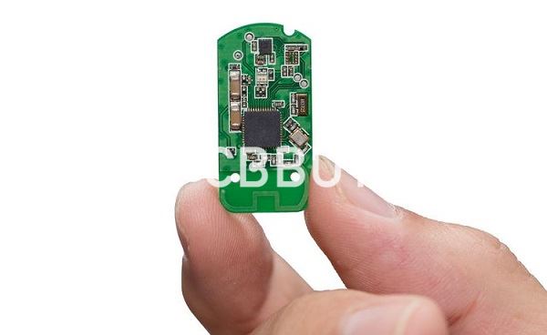
· Board size (LxW): At the end of the day, your PCB will have to be cut from a larger slab of material. For single board processing, the minimum size of the longest edge of a single board acceptable by most manufacturer conveyors is 2.0”. For smaller boards, panelization is typically required.
· Number of layers: The more layers you have the more your board will cost. 1-2 layers is pretty standard, with some manufacturers going as high as 20 layers or more.
· Thickness: Generally, there are thickness requirements associated with the board itself and its individual inner layers. 0.020” of inner layer clearance is pretty standard, with premiums available for tighter tolerances.
3. What is the PCB manufacturing panel dimension?
When a printed circuit board is constructed, using the standard PCB panel size makes work lighter and faster. Remember the two most used methods of PCB penalization we talked about pointed out in chapter one? They both have different reactions to the fabrication panel size of a circuit board. By this, I mean their efficiencies vary concerning the PCB size.

For a standard PCB panel size of 18 by 24 inches, the border clearance needed would not be more than half inches. When the layers increase, the border clearance required also grows with it, so half inches will no longer be sufficient for a standard PCB panel size with multiple layers.
4. How to balance PCB stackup?
Working from the middle layers outward, design the stack-up so that there is a mirror image as you work your way towards the outer layers. It is not always possible to use the same thickness of dielectric and metal layers. It’s important to use thicker copper for power and ground planes. Thicker copper doesn’t readily support etching of fine lines, so our trace layers end up using a thinner sheet of copper. In practical terms, we’re actually designing the space between the copper because that is what is being removed during the fabrication process.
It's also important to note, the outer layers will have to be plated up in order to plate copper into the barrels of the vias. In most cases, a fabrication shop has to create a core via for sequential lamination, the outer layers that make up the span of the core via may have to be treated as if they were outer layers for the same reason. Stacking the micro-vias may invoke a minimum copper weight. When you’re doing these complex high density interconnect (HDI) constructions, don’t go it alone. Make sure your vendor can actually build the board based on the stack-up, line-width, and air-gap goals.
5. How to select PCB substrate dimension?
The PCB substrate is an insulating material typically only millimeters thick. One of the most important decisions in PCB design is deciding how large to make the lateral dimensions of the board. The lateral dimensions of a PCB are often limited by the final device casing it will be placed in, the size of electrical components to be placed on the board, and the width of the copper tracks.

6. What is the standard of PCB board dimension tolerance?
Our standard mechanical tolerances are:
PCB Contour
Dimension +/- 0.20mm
Positional +/- 0.20mm
Cut-out
Dimension +/- 0.20mm
Positional +/- 0.20mm
Slot
Dimension
Length +/-0.20mm
Width +/-0.20mm
Positional +/-0.20mm
Industry Category


