Top 6 Main Features of PCB Substrate Material Properties
By:PCBBUY 10/26/2021 09:28

If your goal is to design a suitable circuit, you also need to consider how rough the copper foil surface will be. Roughing will ensure that the conductors have peel strength and that bonding of the substrate material and the copper foil is optimal. The standard roughness nowadays is set to around 5μm.
In this passage, you could learn 7 main features about PCB Substrate. If you are interested in PCB substrate, please check and read the content below for more information.
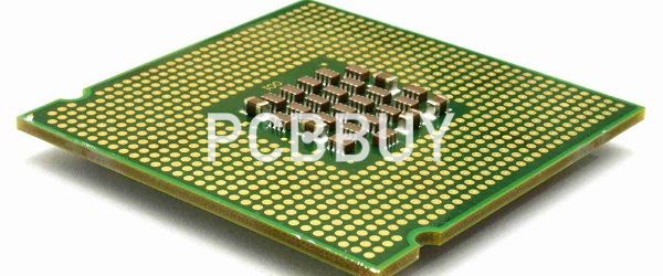
What are the types of PCB substrate?
Once upon a time, the choice in radio frequency/microwave circuit-board materials was a simple choice of:
· Hard, or rigid circuit material
· Soft, or flexible circuit material
You now have more to choose from. With the boom in electronics, circuit materials are now available for specific applications, such as antennas, or even frequency ranges, e.g. millimeter-wave frequencies.
Still, the base substrate for most PCB materials tends to fall into the same categories as before: hard/rigid or soft/flexible.
What are the 6 main features about PCB substrate?
1. Mechanical properties of copper tube and the matrix resin adhesion (peel strength) and mechanical strength (e.g., flexural strength), impact resistance, dimensional stability, flexibility, heat distortion resistance, the base processing (punching, drilling performance) and the like.
2. Electrical characteristics of insulation resistance, resistance to the electric field strength (voltage resistance), the dielectric properties (dielectric constant, dielectric loss factor Wei, etc.), ion migration resistance, resistance to leakage and trace quality copper resistance.
3. The physical characteristics of thermal expansion coefficient (CTE), flammability (flame retardant), a base that is generally warped by the degree of flatness (bow and twist), moisture absorption.
4. Chemical properties. Heat resistance, breaking glass transition temperature (Tg), weldability, resistance to chemicals capacity (acid, alkali and solvent resistance) and the like.
5. Environmental resistance. Fungus resistance, moisture resistance, cooking, resistance to thermal shock properties.
6. Green living substrates suitable for RoHS Directive inauspicious lead and other harmful substances halogen chapter though - .. Some high reliability requirements of the product is not currently required · main lead solder must be used, but from the perspective of environmental protection jealous consideration. When conditions are ripe to make the use of non-polluting or less polluting materials.
What are the properties of PCB substrate?
This material allows a minimum amount of electricity from the circuit. Because there exists an insulating layer between two conducting layers. For example, FR-4 is the most common sort of dielectric substantial. You must consider its properties before choosing it for your circuit board.

Here are the 4 most important properties of dielectric material:
Thermal Properties
Let’s consider the thermal properties of the substrate material:
A temperature range in which a glassy or rigid state of the PCB substrate becomes a softened or deformable state. The properties of the material return its original states after cooling down. You can express this temperature range in the Tg unit. And, you need to measure this temperature in degrees Celsius.
Electrical properties
Relative Permittivity of Dielectric Constant (Dk or Er)
It is very important to consider the dielectric constant of material for checking impedance considerations and signal integrity. Both are remarkable factors of high-frequency electrical performance. The range of Er is between 2.5 and 4.5 in most PCB substrate material.
Chemical Properties
Flammability Specs – UL94
It is a plastics flammability standard for classifying plastic from the lowest flame-retardant to the highest one. So it is very helpful for plastic material appliances testing. Underwriters Laboratories (UL) defines this standard. Here are some essential requirements of this standard:
· Mechanical Properties
· Peel Strength
It denotes the bond strength between the dielectric material and copper conductor. The unit to express the peel strength is pounds of force per linear inch. You can denote it as PLI.
· Thermal Stress: After floating the sample on solder for 10s at 288 ºC.
· Elevated Temperature: After exposing the sample to the fluid at 125 ºC. Or, you can expose that to hot air.
· Exposure to Process Chemicals: After exposing the sample to a series of chemical and thermal processes.
Industry Category


