Understanding HDI Technology in PCB Manufacturing
By:PCBBUY 06/09/2025 13:50
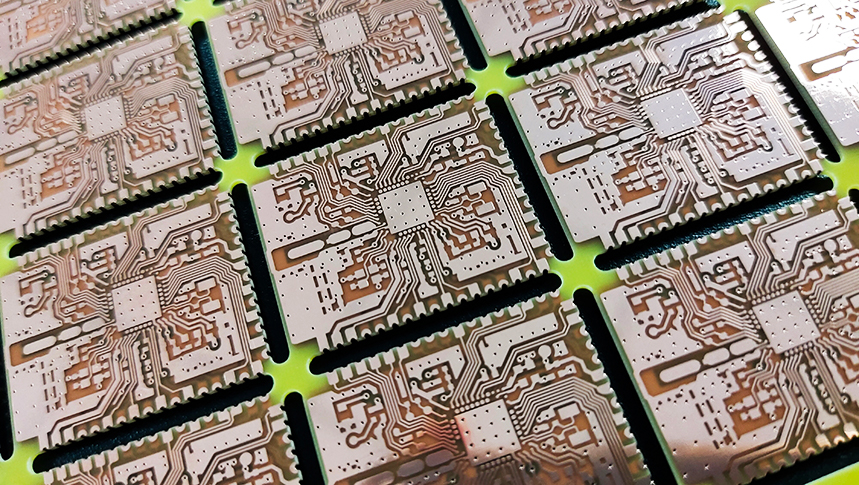
HDI (High-Density Interconnect) technology represents the cutting-edge of PCB innovation. With finer lines, smaller vias, and higher wiring density, HDI PCBs support advanced electronics with compact form factors, fast signal transmission, and high functionality. At PCBBUY, we leverage industry-leading HDI processes to provide customers with robust solutions for complex circuit designs.
What is HDI Technology?
HDI Technology refers to printed circuit boards that use microvias, fine lines, and high-density layouts to achieve greater circuit density per unit area. Compared with traditional PCBs, HDI PCBs contain one or more “build-up” layers, using advanced lamination and via drilling techniques (mechanical and laser drilling). These designs enable miniaturization, better electrical performance, and improved signal integrity.
Key features include:
-
Microvias (≤ 0.15mm for mechanical, ≥ 0.075mm for laser)
-
High aspect ratio holes
-
Laser via electroplating with depth 0.05–0.1mm and ±15% tolerance
-
Construction types like 1+N+1, 2+N+2, etc.
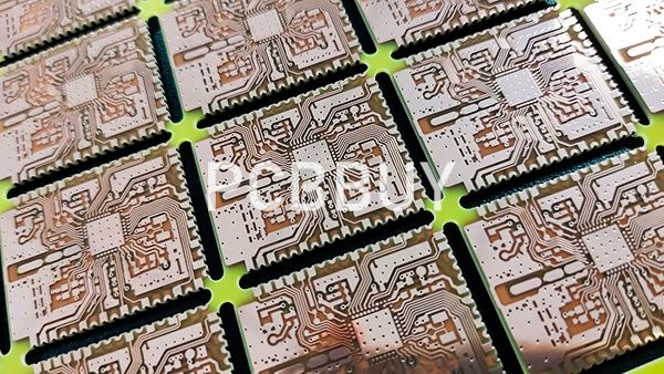
What Is HDI Technology Production Process?
The HDI manufacturing process is significantly more complex than standard PCBs. It includes multiple lamination cycles, precise drilling, and advanced plating techniques.
Step 1: Core Board Fabrication
The inner core is manufactured first with traditional etching and drilling processes to form base signal layers.
Step 2: Laser Drilling Microvias
A laser drill is used to create microvias—typically 75–150 μm in diameter. These are essential for layer-to-layer connections in HDI stack-ups.
Step 3: Copper Deposition
Laser-drilled vias are plated with copper using direct metallization or electroless/electrolytic copper plating to ensure conductivity.
Step 4: Build-Up Layers
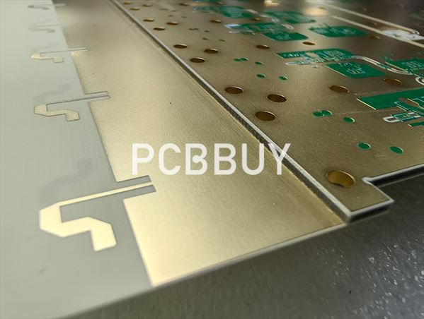
Using sequential lamination, insulating layers and additional copper foils are stacked and bonded. The process may repeat several times depending on the complexity (e.g., 1+N+1, 2+N+2).
Step 5: Via Filling
Via holes are filled with copper or conductive paste to allow for via-in-pad designs and flat surfaces.
Step 6: Fine Line Imaging & Etching
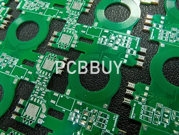
HDI PCBs require ultra-fine trace widths and spacings. LDI (Laser Direct Imaging) is often used for precision imaging before etching.
Step 7: Final Finishing
Processes such as solder mask application, surface finish (ENIG, OSP), routing, and testing are performed to complete the board.
What Are Capabilities and Standards HDI Technology?
At PCBBUY, we offer a complete suite of HDI capabilities to match your product specifications.
|
Item |
Standard |
PCBBUY HDI Technology Highlights |
|
Material |
FR-4, TG135-TG170 |
Halogen-free, CTI customizable |
|
Layers |
4–10 layers (1st), 6–10 layers (2nd) |
Custom stack-up supported |
|
Construction Type |
1+N+1, 2+N+2, 3+N+3 |
Multi-order buildup, n buried vias ≤ 0.3mm |
|
Trace Width |
2/2mil (min) |
High resolution circuit pattern |
|
Blind Via |
Mechanical ≥0.15mm, Laser ≥0.075mm |
Review needed for specification |
|
Hole Size |
Min unilateral ≥3mil |
Small precision drillings |
|
Hole Copper |
>18μm (no blind), >13μm (laser blind) |
Customized per design |
|
Via Electroplating |
Depth 0.05–0.1mm, tolerance ±15% |
Ensures full metalization of via |
Our team also supports electroplating via filling and mechanical structuring, depending on customer design documents and stack-up plans.
Q&A: Common Challenges in HDI Technology Manufacturing
Q1: Why is microvia drilling a challenge in HDI technology manufacturing?
A1: HDI PCBs require microvias with diameters as small as 75–150 μm, which must be drilled using high-precision laser equipment. Any misalignment or depth inaccuracy can compromise the electrical connection or cause defects such as open vias and poor plating.
Q2: What difficulties arise from multiple lamination cycles in HDI technology?
A2: Sequential lamination is a core part of HDI production. Each cycle adds more layers, increasing the risk of layer misregistration, delamination, and internal stress. Precise alignment and strict process control are required to maintain structural integrity.
Q3: How does via filling impact the quality of HDI PCBs?
A3: Via filling, especially for via-in-pad designs, must be uniform and complete. Incomplete filling can cause poor solder joints or electrical disconnection. Copper or conductive paste is used, and inconsistencies during filling or curing can affect reliability.
Q4: Why is it hard to image fine lines in HDI PCB production?
A4: HDI boards often require ultra-fine lines/spaces down to 2/2mil or even smaller. Achieving this requires advanced imaging technology such as Laser Direct Imaging (LDI). Even minor contamination or misalignment can lead to shorts or open circuits.
Q5: What thermal issues must be managed in HDI PCB manufacturing?
A5: The sequential lamination and soldering processes expose HDI boards to repeated thermal cycles. If not managed properly, these cycles can lead to via cracking, material expansion, or delamination. High-quality materials and optimized profiles are essential.
Q6: Why are HDI PCBs more expensive and lower-yielding than traditional boards?
A6: The advanced techniques used in HDI manufacturing—laser drilling, sequential lamination, fine-line etching—are costly and complex. Yield rates are lower due to the tight tolerances and increased risk of defects, especially in higher-order HDI types like 3+N+3.
Q7: How does PCBBUY address these HDI manufacturing challenges?
A7: PCBBUY employs state-of-the-art equipment, experienced engineers, and strict quality control at each step of the HDI process. Our DFM review helps reduce defect risks early in the design stage, and we offer full support for advanced HDI structures.
Conclusion
HDI Technology is essential for next-generation electronics, combining density, performance, and miniaturization. With PCBBUY’s professional HDI PCB manufacturing services, your innovative designs can move quickly from layout to production—optimized for speed, accuracy, and function.
Industry Category


