Via-in-Pad Feasibility for 8 Layer PCB Manufacturing
By:PCBBUY 01/23/2026 15:47
Introduction
As electronic products continue to evolve toward higher density and smaller form factors, via-in-pad (VIP) technology has become an important solution for routing constraints under fine-pitch components. When applied to multilayer designs, especially 8 layer PCB, evaluating the via-in-pad feasibility becomes critical due to increased complexity in lamination, drilling, plating, and reliability control.
This article explores the technical feasibility of via-in-pad in 8 layer PCB designs and explains the manufacturing capabilities required to produce reliable results.
What Is Via-in-Pad Technology?
Via-in-pad technology places a via directly inside a component pad, allowing signals to transition between layers without consuming additional routing space. Compared to traditional dog-bone fan-out structures, via-in-pad enables:
-
Higher routing density
-
Shorter signal paths
-
Improved electrical performance
However, via-in-pad requires advanced manufacturing processes to prevent solder wicking and surface irregularities.
Why Via-in-Pad Feasibility Is Critical in 8 Layer PCB?
In 8 layer PCB designs, via-in-pad feasibility is affected by several factors:
-
Increased board thickness and via aspect ratio
-
Multiple lamination interfaces
-
Higher thermal stress during assembly
-
Stricter flatness requirements for component soldering
Without proper process control, via-in-pad structures may lead to assembly defects or long-term reliability issues.
Types of Via-in-Pad Structures Used in 8 Layer PCB
Via-in-Pad Plated Over (VIPPO)
The via is filled and then capped with copper, creating a flat surface suitable for fine-pitch components.
Filled and Capped Vias
Vias may be filled with conductive or non-conductive materials before copper capping to prevent solder wicking.
Blind Via-in-Pad
Often used to reduce aspect ratio and improve reliability by limiting via depth.
Each structure has different manufacturing and reliability implications.
Via Filling Materials and Processes
Via filling is a key step in via-in-pad manufacturing. Common approaches include:
-
Non-conductive resin filling, widely used for stability and cost efficiency
-
Copper filling, offering superior electrical and thermal performance
After filling, planarization ensures a smooth and flat pad surface for soldering.
Manufacturing Challenges Affecting Via-in-Pad Feasibility
Several process challenges must be controlled to ensure via-in-pad feasibility in 8 layer PCB:
-
Void-free via filling
-
Uniform copper capping thickness
-
Surface flatness control
-
Reliable bonding during lamination
These challenges require advanced equipment and experienced process engineering.
Impact of Via-in-Pad on Reliability
Properly manufactured via-in-pad structures improve reliability by:
-
Eliminating solder wicking
-
Reducing thermal stress concentration
-
Enhancing electrical continuity
Poorly controlled via-in-pad, however, can lead to cracks, delamination, or intermittent connections during thermal cycling.
Design Guidelines for Via-in-Pad in 8 Layer PCB
To improve manufacturability and reliability, designers should consider:
-
Limiting via aspect ratio
-
Selecting appropriate via diameters and pad sizes
-
Using blind vias when feasible
-
Communicating stackup and via requirements early
Design-for-manufacturing collaboration is essential for successful via-in-pad implementation.
Inspection and Quality Control for Via-in-Pad
Manufacturers use multiple inspection methods to verify via-in-pad quality:
-
X-ray inspection to detect voids
-
Micro-section analysis to examine via structure
-
Surface flatness measurement
These inspections ensure via-in-pad structures meet assembly and reliability standards.
Manufacturing Capability Required for Via-in-Pad in 8 Layer PCB
Successful via-in-pad production requires:
-
Precision drilling and via filling equipment
-
Stable copper plating and planarization processes
-
Controlled multilayer lamination
-
Experienced engineering support for feasibility review
These capabilities are critical for complex multilayer PCB manufacturing.
Typical Applications Using Via-in-Pad in 8 Layer PCB
Via-in-pad technology is commonly applied in:
-
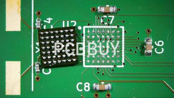
Fine-pitch BGA and CSP packages
-
High-speed digital systems
-
Communication and networking equipment
-
Compact industrial electronics
Conclusion
Via-in-pad feasibility for 8 layer PCB depends on a combination of thoughtful design and advanced manufacturing capability. From via filling and copper capping to lamination and inspection, each process step must be carefully controlled to ensure long-term reliability.
Manufacturers with strong via-in-pad expertise can support high-density 8 layer PCB designs that meet both electrical and mechanical performance requirements.
Industry Category


