What Are Gold Fingers PCB and How Does It Made?
By:PCBBUY 12/23/2021 09:34

There are some standards you need to follow for the gold fingers so that it can work correctly during the plating process of gold finger. As well as the PCB design need to take into account the areas where is necessary to proper finger length and alignment. Gold is chosen for these fingers as it has the highest corrosion resistance and electrical conductivity after Copper and Silver.
If you are a beginner of PCB industry, please check and read the content blow in this passage for more information of gold gingers PCB. Do you know what gold gingers PCB is? Do you know how to make it?If you are going to learn more knowledge about it, let’s go for the passage.
How are gold fingers applied?
Gold fingers can be used for many various things. And they use depending on the designer’s purpose. There are some common applications of gold fingers as the follows:
1. Provide an interconnection point for transferring network data;
2. Connect external components to the PCB prototype;
3. A place for attaching specialized adapters or daughter boards;
4. Serve as an audio adapter
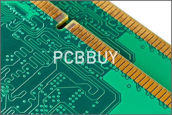
What is PCB gold finger beveling?
Have you found out that the edges of PCB gold fingers are in slope forms? Well, the procedure of beveling allows sharp, square edges to turn into slopes. In the case of PCBs or printed circuit boards, the beveling process completes the surface finish. The beveling process of the gold fingers of a PCB gets initiated after completing the disposition of solder masks. The process of PCB gold finger beveling is unavoidable in terms of making insertions quicker and more effortless. Unless the gold finger beveling is completed, insertions will be more difficult than usual.
As you have already known about the beveling process, you also have to know which angle you are supposed to bevel the edges. Usually, PCB gold fingers are beveled at angles of 30 or 45 degrees to ease up the particular slot’s insertion process. Anyway, engineers and technicians bevel PCB gold fingers according to the requirements of the clients. The beveling angle of gold fingers also depends on the size of a particular circuit board.

What are the standards of PCB gold finger?
The production standards for PCB gold fingers were established in 2002 by the Association Connecting Electronics Industries (IPC). The standards were amended in 2012 with the release of IPC-4556. In 2015, the standards were again amended with the release of IPC A-600 and IPC-6010, which are currently the most widely employed standards in PCB production. The IPC standards can be summarized as follows:
Chemical composition:
For maximum rigidity along the edges of PCB contacts, the gold plating should consist of between 5 and 10 percent cobalt.
Thickness:
The plating thickness of gold fingers should always fall within the range of 2 to 50 microinches. The standard thicknesses by size are 0.031 inches, 0.062 inches, 0.093 inches and 0.125 inches. The lower thicknesses are generally used for prototypes while the higher thicknesses are used along connecting edges that are regularly inserted, unplugged and reinserted.
Visual test:
Gold fingers should pass a visual test conducted with a magnifying lens. The edges should have a smooth, clean surface and be free of excess plating or the appearance of nickel.
Tape test:
To test the adhesiveness of the gold plating along with the contacts, the ICP recommends a test whereby a strip of tape is placed along the contact edges. After removing the tape, inspect the strip for traces of plating. If any gold plating is evident on the tape, the plating lacks sufficient adhesiveness along with the contacts.
Numerous other standards exist for the PCB gold finger plating process, and all should be read in full for an in-depth understanding. As technology improves, further standards of testing are commonly introduced to the process, so it is best to check back with the IPC for updates periodically.

What are the applications of PCB gold finger?
As mentioned above, the interactions between the circuit boards and motherboards of different devices are essential for better connectivity. Along with the rapid development of technology, smartphones, PCs, and other devices tend to be faster and more advanced. As technology and connectivity are getting smarter, the importance and significance of PCB gold fingers are increasing. Gold-plated circuit boards are what made the technology as smart as it is currently. With the advancement of time, technology keeps getting more improved and faster. That’s happening due to the improved versions of gold-plated circuit boards.
The gold fingers of a circuit board allow insertion and ejection easier and faster. From smartphones to other smart devices, everything is dependent on the functions of the gold fingers. The advancement of gold fingers of PCBs and the enhancement in their performances are what can take the improvement of the smart technology to the next level. The advanced and improved versions of gold fingers enhance the performances of printed circuit boards of different devices. Therefore, it can be said that the gold fingers are liable for the incredible up-gradation of smart technology, and it is changing the global digital trend effectively.
Industry Category


