What Are PCB Best Practices for Avoiding Crosstalk?
By:PCBBUY 08/28/2024 17:26
Crosstalk is a common and often problematic issue in printed circuit board (PCB) design, especially as electronic devices become more compact and operate at higher frequencies. It occurs when a signal transmitted on one circuit or channel creates an undesired effect on another circuit or channel. This unintended coupling can lead to noise, interference, and degradation of signal integrity, potentially causing devices to malfunction. Understanding how to avoid crosstalk is essential for engineers designing PCBs that meet performance and reliability standards. This article delves into the best practices for avoiding crosstalk in PCB design, supported by professional industry knowledge, data, equations, and tables.
Definition and Causes
Crosstalk refers to the electromagnetic interference that occurs when a signal from one PCB trace or wire unintentionally affects another nearby trace or wire. This phenomenon is primarily due to capacitive coupling and inductive coupling:
Capacitive Coupling: When two conductors are close to each other, an electric field can develop between them, causing signal interference. The coupling is more pronounced with high-frequency signals, where electric field changes are rapid.
Inductive Coupling: This occurs when a varying current in one conductor creates a magnetic field that induces a voltage in a nearby conductor. The higher the frequency and the closer the conductors, the stronger the inductive coupling.
These couplings can lead to noise and signal distortion, which may affect the performance of the entire circuit. High-speed digital circuits, radio frequency (RF) circuits, and mixed-signal designs are particularly susceptible to crosstalk.
Effects of Crosstalk
Crosstalk can have several detrimental effects on PCB performance, including:
Signal Integrity Degradation: Crosstalk can cause unwanted noise and signal degradation, leading to errors in data transmission and processing.
Increased Electromagnetic Interference (EMI): Crosstalk can contribute to EMI, which can interfere with other components or systems.
Timing Issues: In high-speed circuits, crosstalk can lead to timing errors, causing the circuit to malfunction.
Key Parameters Influencing Crosstalk
Several parameters can influence the level of crosstalk in PCB designs:
Trace Spacing
The distance between traces is a critical factor. Closer traces result in stronger capacitive and inductive coupling.
Trace Width and Height
Wider traces have more surface area, which can lead to increased capacitive coupling. The height of traces from the ground plane also affects crosstalk levels.
Dielectric Material
The dielectric constant of the material between traces influences capacitive coupling. Materials with higher dielectric constants increase the coupling and hence the crosstalk.
Frequency of Operation
Higher frequency signals are more susceptible to crosstalk due to the increased rate of change of electric and magnetic fields.
Signal Rise Time
Faster rise times (sharp transitions from low to high voltage) in digital signals can exacerbate crosstalk, as they contain higher frequency components.
Best Practices for Avoiding Crosstalk
To minimize crosstalk in PCB designs, several best practices can be followed. These practices involve careful layout planning, signal routing, and the use of appropriate materials and design techniques.
Increase Trace Spacing
Guideline: Keep a minimum distance of 3 times the trace width between adjacent signal traces to reduce capacitive coupling.
Justification: Increasing the spacing between traces reduces the electric field interaction between them, effectively lowering the capacitive coupling and the resultant crosstalk.
Equation:

Increasing the spacing (distance) reduces the proportional crosstalk.
Use Ground Planes
Guideline: Place continuous ground planes directly beneath signal traces.
Justification: Ground planes help to shield signals, reducing the coupling between traces. They also provide a low impedance return path, which helps in minimizing inductive coupling.
Differential Pair Routing
Guideline: For high-speed and sensitive signals, use differential pairs.
Justification: Differential pairs help to cancel out the noise and reduce the impact of crosstalk by carrying equal and opposite signals. The induced noise affects both lines equally, thus getting canceled at the receiver end.
Control the Signal Rise Time
Guideline: Use signal drivers with controlled rise times for high-speed signals.
Justification: Reducing the rise time of signals can lower high-frequency content, which in turn reduces crosstalk.
Minimize Parallel Routing Lengths
Guideline: Avoid long parallel runs of traces; if unavoidable, stagger or zigzag them to minimize coupling.
Justification: Long parallel traces increase the likelihood of crosstalk. By staggering the routing, the coupling distance changes, reducing overall interference.
Use Guard Traces
Guideline: Place guard traces between sensitive signal lines.
Justification: Guard traces are grounded traces placed between signal lines to absorb interference. They act as shields and reduce the coupling between signal traces.
Equation for Guard Trace Effectiveness:

Where d1 is the distance between the signal trace and the guard trace, and d2 is the distance between the signal trace and the adjacent trace.
Use Proper Termination
Guideline: Implement proper termination techniques for high-speed signals.
Justification: Proper termination prevents signal reflections, which can interact with other signals, leading to crosstalk. Termination resistors matched to the trace impedance can help in reducing these reflections.

Advanced Techniques for Reducing Crosstalk
Layer Stackup Design
Guideline: Design multi-layer PCBs with a proper layer stackup, ensuring that signal layers are adjacent to ground or power planes.
Justification: A well-designed stackup with alternating signal and ground layers minimizes the loop area and reduces crosstalk. The ground planes act as shields and provide return paths, reducing the loop inductance.
Example Stackup:
|
Layer |
Description |
|
1 |
Signal Layer |
|
2 |
Ground Plane |
|
3 |
Ground Plane |
|
4 |
Ground Plane |
Crosstalk Simulation
Guideline: Use PCB simulation tools to predict and analyze crosstalk during the design phase.
Justification: Simulation tools can model electromagnetic fields and predict crosstalk effects, allowing designers to make informed decisions before manufacturing. Simulations can provide data on how changes in trace spacing, layer stackup, and routing strategies impact crosstalk.
Case Studies and Data Analysis
Case Study 1: Impact of Trace Spacing on Crosstalk
A study conducted on a 4-layer PCB design showed that increasing the trace spacing from 4 mils to 10 mils reduced crosstalk by 30%. This significant reduction illustrates the effectiveness of trace spacing as a primary means of controlling crosstalk.
|
Trace Spacing (mils) |
Crosstalk Level (mV) |
|
4 |
120 |
|
6 |
90 |
|
8 |
70 |
|
10 |
50 |
Case Study 2: Use of Guard Traces
Introducing a grounded guard trace between two high-speed signal traces resulted in a 15 dB reduction in crosstalk. This case study emphasizes the value of guard traces, especially in high-density PCB designs where increasing trace spacing is not feasible.
Theoretical Analysis
Capacitance and Inductance Models
Capacitance and inductance between traces can be modeled using equations to estimate crosstalk. For example, the mutual capacitance \( C_m \) and mutual inductance \( L_m \) can be calculated using:
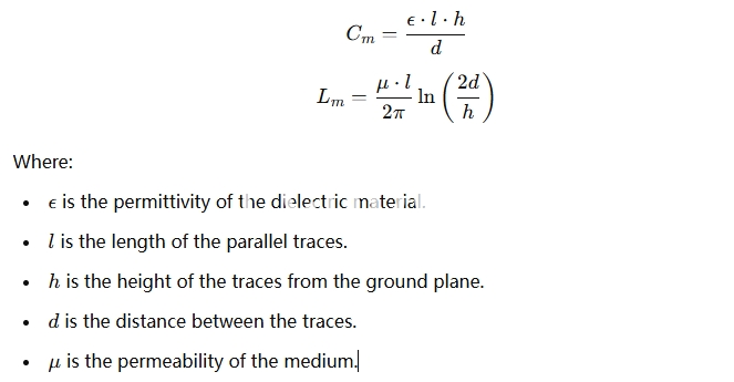
These equations provide insights into how physical parameters affect crosstalk and guide design choices.
Practical Tips for PCB Designers
1. Review Design Guidelines: Regularly update and follow design guidelines specific to the application to minimize crosstalk.
2. Simulate Before Fabrication: Use simulation tools to test for crosstalk and make necessary adjustments before manufacturing.
3. Use High-Quality Materials: Select materials with appropriate dielectric properties that reduce capacitive coupling.
4. Consult with Manufacturers: Work closely with PCB manufacturers
Conclusion
Crosstalk is a significant concern in PCB design, especially with the ongoing trend towards miniaturization and high-speed signal processing. By following the best practices outlined in this article, such as increasing trace spacing, using ground planes, employing differential pair routing, and utilizing simulation tools, designers can effectively minimize crosstalk and enhance the performance and reliability of their PCBs. A proactive approach to crosstalk mitigation not only ensures compliance with industry standards but also significantly reduces the likelihood of costly redesigns and field failures.
References
1. Howard Johnson, Martin Graham (2003). "High-Speed Digital Design: A Handbook of Black Magic". Prentice Hall.
2. IPC-2221: Generic Standard on Printed Board Design.
3. IPC-2141A: Design Guide for High-Speed Controlled Impedance Circuit Boards and Assemblies.
4. Ralph Morrison (2016). "Grounding and Shielding: Circuits and Interference". Wiley-IEEE Press.
5. Eric Bogatin (2009). "Signal and Power Integrity - Simplified". Prentice Hall.
Industry Category


