What Are PCB Pads and What Are the Functions?
By:PCBBUY 12/14/2021 09:39

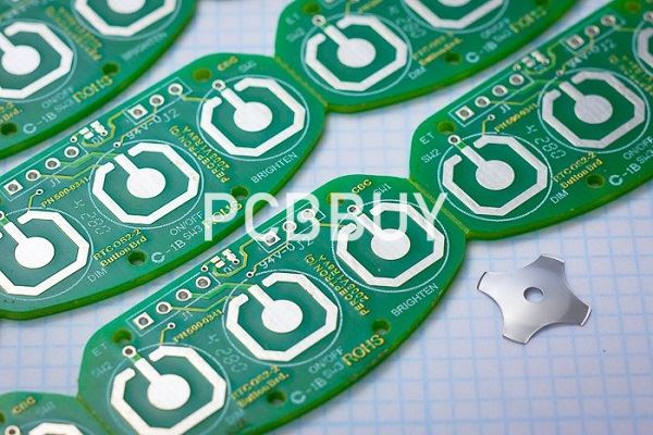
A pad is the exposed region of metal on a circuit board that the component lead is soldered to. Multiple pads in conjunction are used to generate the component footprint or land pattern on the PCB. The two types of pads available are through-hole and surface mount pads.
Are you a beginner of PCB industry? If you are looking for more details information of PCB Pads, please check and read the content the content below in this passage.
What are the considerations of PCB Pads?
Ensuring a PCB pad stack design meets manufacturability and reliability requirements needs one to consider several factors:
· Maximum tolerances build up the minimum insulation between opposing conductors, which in this case refers to the hole plating and the copper in the trace and plane layers. They need to comply with the standards of the engineered product. For telecommunication equipment, a minimum insulation spacing of 4 mils is required and for other products it is 5 mils.
· There need to be robust connections between traces and plated through-holes or vias.
· The aspect ratio needs to be such that the hole wall should withstand the stress of the plating process without failure.
Even if you follow the guidelines above, drilled holes might not always pass through the board as specified. This might happen due to the following factors:
· Drill wander can occur where the drill can deviate from the preferred drilling axis (eccentricity)
· Alignment errors in the film layers
· Laminate shrinkage during lamination. This might lead to an error in locating the drill hole.
· Inaccurate registration of the layers during lamination
What are the standards of PCB Pads?
First of all, let’s define exactly what a “pad” is. A pad, also known as a “land,” is the exposed area of metal on a circuit board that the lead of a part will be soldered to. Multiple pads are used to create the component footprint, or land pattern, on the printed circuit board.
This process could be very error-prone, however, as manufacturers’ specifications didn’t always adhere to the same formulas. This could result in layout designers using the wrong sizes and shapes in their pads. These incorrect pad sizes and shapes, unfortunately, could have disastrous consequences during manufacturing, including:

Through-hole breakout
Through-hole pads must have a solid annular ring for solderability, which is the metal between the hole wall and the outer perimeter of the pad. The annular ring specification is designed to be large enough to allow for the expected amount of drill wandering from the center of the hole. If the pad is too small, however, there could be some breakout of the annular ring, and too much breakout can result in improper soldering or broken and incomplete circuits.
Insufficient solder joints
SMT parts that have too small of pads run the risk of not getting a proper solder fillet during manufacturing. Without a good fillet, the solder joint will be weak and can break.
Floating parts
SMT parts that are soldered to pads that are too large could end up floating out of position during solder reflow. This can cause conflicts with other parts or even shorts between circuits.
Tombstoning parts
Smaller two pinned SMT parts, like resistors and capacitors, can have problems soldering if their pads are not the same size. One pad will heat faster than the other, and the melting solder will pull the part up and away from the other pad, sticking up like a tombstone.
What are the features of surface mount pads?
Surface mount pads have the following features:
· These pads are of copper;
· They can be rectangular, round, elliptical, or square;
· Solder mask layer;
· Solder paste;
· Pad number (quantity of pads show for the part)
· Exceptional characteristics of BGA pad#
· SMD pad vs. NSMD pad
· The PCB thermal pad to control the temperature of solder joints
Correct pad pattern is vital to assure the manufacturability of BGA factors. In that respect, there are fundamentally two sorts of BGA pads. They are the non-solder mask defined pad (NSMD) and the solder mask defined pad (SMD).

Non-solder mask defined pads change from solder masks defined pads (SMD pads) in that the solder mask is specified not to touch the copper area. The mask is alternatively produced, determined that a break is begotten between the pad adjoin and the solder mask.
SMD pads are specified by the solder mask apertures enforced to the BGA pads. SMD pads have the solder mask aperture defined that the mask initiatory is more pocket-sized than the diameter of the pad they address. This is made out to contract the copper pad sizing that the component will be soldered to.
Industry Category


