What Are Vias in PCB Design & What Are the Differences among Them?
By:PCBBUY 01/06/2022 09:31

A via is a plated-through hole in a PCB that you can use to route a trace from your board's surface layer to the inner and other layers. It is essential to realize that you can drill PCB vias mechanically, and you can plate them to create electrical connections.
Do you know all the detailed knowledge about vias in PCB? If you are going to learn more information about vias in PCB, please check and read the content below in this passage.
Wanna know PCB knowledge? Check and read for more.
What are the benefits of PCB via?
Because PCBs have limited amounts of space, blind and buried vias can be a huge benefit. They allow you to keep the PCB small, which is essential when working with electronics. The use of vias frees up space on the surface of the board; that space can then be used for other functions. Vias are a relatively simple solution, but you will need to be aware that the addition of blind and buried vias will add to the cost of the board.
Because there are many factors that go into getting the right PCBs with the correct blind and buried vias, it is important to work with a quality manufacturer.
What are the main types of vias in PCB?
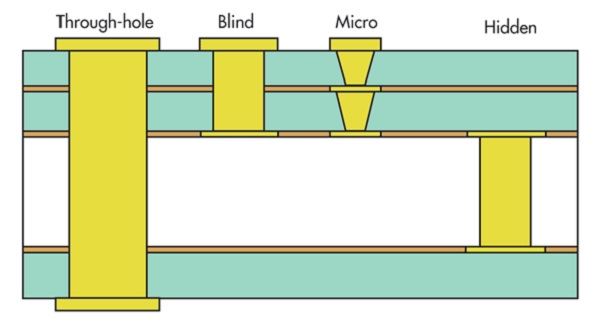
Through-hole vias
The hole penetrates from the top layer to the bottom layer. They can be either PTH or NPTH. For PTH, the connection is established from the top to the bottom layer.
Blind Vias
The hole penetrates from an exterior layer and ends at an interior layer. Here, the hole doesn’t penetrate through the entire board but connects the PCB’s exterior layers to at least one interior layer. Either the connection is from the top layer to a layer in the center or from the bottom layer to some layer in the interior region. The other end of the hole cannot be seen once the lamination is done. Hence, they are called blind vias.
Buried Vias (hidden vias)
These vias are located in the interior region of the PCB. The buried vias have no paths to the outer layers. They connect the inner layers and stay hidden from sight. As per IPC standards, buried vias and blind vias must be 6 mils (150 micrometers) in diameter or less.
Microvias
The most commonly known vias are the microvias (µvias). During PCB manufacturing, microvias are drilled by lasers and have a smaller diameter compared to the standard through-hole vias. Microvias are generally implemented in High-Density Interconnection (HDI) PCBs. The depth of a microvia isn’t usually more than two layers deep since the plating of copper inside these small vias is a tedious task. The smaller the diameter of a via, the higher should be the throwing power of the plating bath to achieve electroless copper plating.
Microvias can be classified into stacked vias and staggered vias based on their location in the PCB layers.
· Stacked vias are piled on top of one another in different layers.
· Staggered vias are scattered in the different layers. And they are more expensive.
· Additionally, there is another type of microvias called skipvias. Skipvias skip one layer, meaning, they pass through a layer making no electrical contact with that specific layer. The skipped layer will not form an electric connection with that via.
What Size Should Vias Be?
Check with your manufacturer for their minimum drill size and minimum annular ring for the manufacturing process they will use. Typical mechanical drills don’t go much lower than 12 mil in diameter without frequent breakage, so the manufacturer will increase the cost to account for broken drills. Annular rings don’t often go below 6 mil for standard processing. So the smallest via you would create has a 12-mil diameter hole, and a 24-mil diameter pad.
What are the considerations of vias in PCB?
Before a PCB layout designer can start dropping vias into their board design, there are a few more details about vias to be discussed. We’ve already talked briefly about the difference in the manufacturing costs between a thru-hole via and a microvia, which can be a real wake-up call if you aren’t prepared for it. Now, here are some other considerations to keep in mind as well.
Aspect Ratio
When using a mechanical drill to create a standard via, it is important to remember that the smallest acceptable drill size is based on how thick the circuit board is. Mechanical drills have a limit to how much material they can drill through before they become unreliable. This is measured by the relationship of board thickness to drill size, and PCB fabricators will usually require an aspect ratio of no more than 10:1 for their drill sizes. This means that for a circuit board that is 62 mils thick, the smallest mechanical drill size that you should use is 6 mils or 0.006 inches. If you need a hole smaller than that, you should look into using microvias which have an aspect ratio of 1:1.
Annular Ring
The size of the via pad is important. You need to ensure that a large enough annular ring remains after the via is drilled. A mechanical drill will wander a little while it is drilling, and without a sufficient annular ring, the via may be compromised by drill breakout.
Signal Integrity
Although a via is very short, it is still a measurable length of the conductor which could cause problems with tight signal integrity requirements. For instance, a thru-hole via that connects the top two layers in a ten layer board will have 8 layers of unnecessary metal in it that could create interference. It is important to find problems like these and remedy them with techniques such as back-drilling the via to remove the unused metal from the line before it acts as an antenna. Here is where the signal integrity analyzers of PCB design tools like Cadence Allegro can be very helpful to the designer in finding these problems before the board goes out for manufacturing.
Industry Category


