What Are the 5 Basic Elements of Plating in PCB Manufacturing Process?
By:PCBBUY 11/25/2021 09:15

As we have seen, printed circuit boards are fabricated with copper features for electrical connectivity. Although the traces and area fills will usually be covered and protected with a solder mask, the pads and holes must be left out in the open for soldering. This exposure will pose a problem because copper left unprotected for any length of time will begin to oxidize and deteriorate, making the circuit board unusable. For this reason, a surface finish is applied or plated onto the exposed copper for its protection.
In this passage, we will provide all the details about PCB plating. If you are curious about the information of PCB plating, please check and read the content below.

How to process PCB plating on surface finish?
Different types of surface finishes can be used on a circuit board depending on what kind of protection the board needs:
HASL (Hot Air Solder Leveling)
Up until recently, HASL has been the most widely used surface finish in the industry. The circuit board would be dipped into a molten pool of solder and then run through hot blasts of air to remove the excess. HASL is a low-cost operation available almost anywhere. It has a long shelf life and is easy to use. The downside of HASL is that it leaves uneven surfaces that can cause solder bridging and are not detailed enough for fine pitch components.
ENIG (Electroless Nickel Immersion Gold)
ENIG has become one of the most popular surface finishes currently being applied to circuit boards. It is composed of two layers of metal coatings, with the first being a layer of nickel that is chemically plated to the board. The nickel provides a barrier of protection for the copper and then, in turn, is protected from oxidation by a thin layer of gold. ENIG has excellent surface planarity making it ideal for soldering fine pitch components. It complies with the Restriction of Hazardous Substances (RoHS) requirements and is durable with a long shelf life. On the other hand, it is more expensive than other finishes, such as HASL.
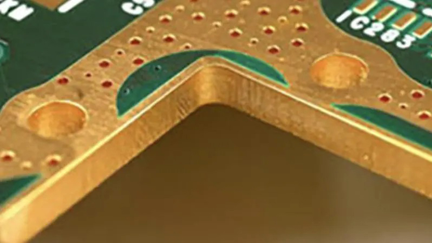
What are the applications of PCB edge plating?
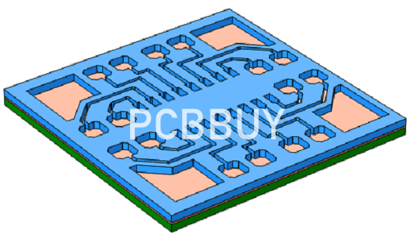
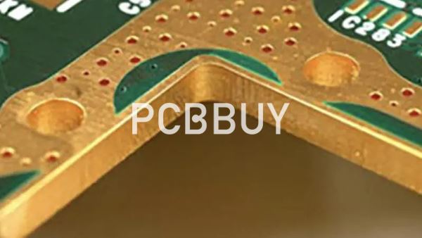
Several industries require edge-plated boards, especially in applications that require better support for connections such as for boards that slide into metal casings. Edge plating has other uses as well as it improves the current-carrying capabilities of the board, provides edge connection and protection, and offers the possibility of edge soldering to improve fabrication.

Although edge plating on printed circuit boards is a simple addition in most cases, fabricators need specialized equipment and trained personnel for the process. Designers must take care that internal power planes do not come up to the edge, and fabricators must make sure there is a gap before they take up edge plating. Designers must make sure there is a band of copper on both edges of the top and bottom side, as the plating will connect to these copper bands.
Now edge plating PCB has been widely used in many industries, particularly in applications that need better support for connections, for example for circuit boards that slide into metal casings. What’s more, edge plating has other benefits as follows:
· Improve the current-carrying capabilities of PCB;
· Offer edge connection and protection;
· Offer the possibility of edge soldering to improve fabrication.
What are the special considerations of PCB plating?
Dissimilar Metal over Metal to Protect Bare Copper
Precious metals are not as easy to obtain or work with but those are the leading partners for plating in today’s consumer market. Gold does not readily bond with copper. Using an intermediate layer of nickel solves this intermetallic issue and is the formula we know best for surface-mount components with via-in-pad technology. Electroless Nickel / Immersion Gold (ENIG) is a very popular finish because it takes to solder really well and does a commendable job of protecting the copper prior to soldering.
When it comes to the stack-ups for flexible printed circuits, the additional plating is normally documented in the stack-up diagram. The added copper stiffens a flex and that may be undesirable. That being the case, we would look into button plating which is more selective than panel plating. As a rule, all plating, masking, covering, marking and stiffening on an FPC is going to be a material designed for that purpose.
For an FPC, the copper itself is annealed, that is to say softened by passing the sheet through two big rollers that squeeze it down again and again. This creates a granular alignment that provides a smooth outer surface for the traces that actually improves signal integrity. It is specified as “rolled annealed copper” or just RA cu. for shorthand.
What are the structures of copper wrap plating?
The IPC 6021B standard has included a copper wrap plating requirement for via-in-pad structures. The filled copper plating should continue around the edge of the via hole and extend onto the annular ring surrounding the via pad. The requirement enhances the reliability of the via plating and can potentially minimize failure due to cracks or separation between the surface features and the plated via-hole.

Filled copper wrap structures are of two types. In one method, a continuous copper film can be applied to the interior of a via which can then wrap over the top and bottom layers at the via ends. This plating will then form the via pad and trace which leads to the via, generating a continuous copper structure.
In another approach the via can have a separate pad formed around the via ends. This separate pad layer is meant to connect to ground planes or traces. The next step would be the copper wrap plating which fills the via and wraps over the top of the external pad, creating a butt joint between the via pad and the copper fill plating. Even though there is a certain extent of bonding between the via pad and the fill plating, the two plating structures do not fuse completely together and form a single continuous structure.
Industry Category


