What Are the 5 Elements of PCB Thermal Management Presentation?
By:PCBBUY 11/24/2021 09:27

In high power density PCB, it is difficult to control heat generation. This occurs because there are many channels of traction power at the same time and many elements that depend on the current supply at the same time. High power density PCBS are not necessarily bad designs; Some applications require high power density to perform various functions. In these cases, the efficient use of space is critical, as any crosstalk may quickly cause a thermal peak.
If you are looking for the information of PCB thermal management, please check and read the passage for more professional knowledge. Come and check the content below.

What is the motivation of PCB thermal management?
The main reason for deficiencies of electrical systems beside dust, vibration and humidity is by far the impact of temperature. Therefore an efficient thermal management concept on the PCB is crucial for the reliability of power electronic systems. As an example we take high power LED applications, which are likely to dominate in the next years residential and commercial lighting, signaling and vehicle headlights due to efficiency and extended lifetime. LEDs that range from 500 milliwatts to as much as 10 watts in a single package have become standard, and researchers expect even higher power in the future.
Thermal management is of critical importance for high power LEDs. More than 60% of the electrical power input is converted into heat and built up at the junctions of LED chips due to non-radiative recombination of electron-hole pairs and low light extraction. If that heat is not removed, the LEDs run at high temperature, which not only lowers their efficiency, but also makes the LED more dangerous, less reliable and shortens operating life. Thus, thermal management of high power LEDs is a crucial area of research and development. In this paper results of simulations and measurements of different LED-modules will be shown and should serve as representative of thermal solutions for general high power applications.
How to identify the PCB thermal management?
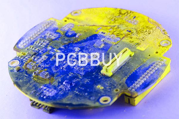
To fabricate a thermally stable PCB, thermal effects must be studied during the designing phase itself. The first step in thermal design is to identify the hotspots. Thermal modeling or thermal simulation techniques are used to find hotspots. Also, current flow analysis must be done along with it, because high-current traces cause heat generation. The proper geometrical arrangement of components and high-current traces enables even distribution of heat. High-current traces must be routed away from thermally sensitive components such as sensors and Op-amps.

The thickness and width of the copper pad or traces play a significant role in PCB thermal design. Copper trace thickness should be adequate to provide a low impedance path for current passing through it. This is because the resistance of copper traces and vias accounts for significant power loss and heat generation particularly when they bear high current density. Therefore sufficient trace width and thickness are recommended to reduce heat generation.
What is the power electronic of PCB thermal management?
Considering most consumer electronic circuits are built on FR4 epoxy circuit board materials, metal core boards compare favorably. They offer an attractive price point and utilize standard assembly processing making possible a near-zero NRE cost of implementations. These metal-core circuit boards, however, have poor thermal dissipation capabilities compared to substrates such as direct-bond copper (DBC). DBC, a stack of copper/alumina/copper, has excellent thermal properties and therefore can be implemented in circuit designs requiring higher thermal load dissipation.
However, DBC is expensive when compared with standard circuit boards and imposes some limitations on circuit design. Advances in thermal management materials can deliver high thermal management performance, excellent physical properties, and be competitively priced while still being compatible with existing circuit manufacturing techniques.
Applied Nanotech (ANI) has developed a group of high-performance graphite-based thermal management materials, known collectively as CarbAl™, and the corresponding surface fictionalization techniques for the purpose of achieving the tough thermal management requirements of power electronic devices. When properly engineered and functionalized, these new concepts in thermal management can maximize performance of heat conduction by:
· Reducing the number of thermally-resistant layers between the device and the environment.
· Reducing the thermal resistance of the layers.
· Using high thermal conductivity materials between each layer of the heat dissipation substrates.

Why thermal relief PCB is important?
Thermal relief plays a vital role while creating your circuit design. You can use the thermal relief pad anytime when you connect the negative plane to the thru-hole part. You know that the thermal relief pad has a varying number of spokes with different width based on how much power requirements are needed for a pin. A power pin, requiring a 40 mil trace and connecting a plane, must have the pad with four 10 mil spokes.
However, the question is- Do your PCB vias need these thermal relief pads. The major reason for using this pad is to maintain a balance of the heat-sinking activities of pins soldered into planes. As the vias do not get the component pin, it does not need any relief pad with thermal properties. It will establish a link to the plane.
Industry Category


