What Are the 5 Tips for Bare PCB Manufacturing Process?
By:PCBBUY 12/31/2021 09:35

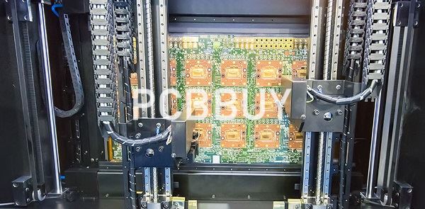
PCB manufacturing is a complicated process where copper layers are etched and hundreds of holes are drilled according to a design. Even with the aid of machines, the results aren’t always perfect. Occasionally, you’ll have issues on a few PCBs that go undetected until they are assembled and deployed.
Do you know bare PCB manufacturing? If you are looking for more information about bare PCB, please check and read the content below in this passage.
1. What is the basic definition of bare PCB?
A bare PCB is a blank board designed for the production of a printed circuit board. This board comprises a metal coating, substrate, and conductive pathways. Bare PCBs boards are available so that engineers can mount electrical components. These boards feature no electrical components. As printed circuit boards are a core material in electronics devices, so is a bare board to a PCB.
A bare board helps the production of several types of PCB. Circuit board manufacturers can’t do anything without this board. A bare PCB is also known as a blank PCB board. Manufacturers mount all electronic components on this board. The bare PCB board provides electrical and mechanical support for circuit production.
2. What are the advantages of bare PCB?
Bare Circuit Boards come with a number of advantages including:
· Saving on Costs - This stand to reason since you are undertaking extensive testing in the initial stages of the design. What you do not have to contend with, therefore are Bare printed circuit boards that are wrongly assembled, which can turn out to be a very costly mistake.
· Saving on time - Once again, since you are identifying issues in the early stages, you don’t tend to lose out on precious time. This can be a huge source of competitive advantage, since this could mean quick time-to-market.
· Easy Resolution - With bare board testing it will be easy to identify and resolve issues early on.
· Reliability - The most important advantage of bare board testing is the reliability that it offers. At a time of miniaturization, boards are extremely densely populated. It is, therefore, important to ensure that your bare board (PCB) is up to soldering the expensive components on it.
Our bare board testing is done vide the Flying Probe Method that works well even for small production volumes and offers affordability as well as flexibility.

3. What is the process of bare PCB manufacturing?
Drilling
Drilling involves the creation of holes for via connections. Here, the foundation for vias is created. This is an important process for the fabrication of bare PCB. The blank PCB drilling process requires serious attention. This is because any error can lead to losses.
Hole Metallization
The already drilled blank PCB boards go through a conveyorized line. Then, the holes are lined with a thin layer of carbon which serves as the cathode.
Photo Mech
This stage involves laminating the drilled bare PCB with photosensitive film plating resist. A direct imaging machine then images the board.
Plating
The manufacturer copper plates the bare printed circuit board. The technique used here is known as periodic pulsed plating. It involves plating copper evenly down small holes and on the tracks’ surface. Manufacturers must take measures to ensure the right amount of copper is in each panel.
Etching
This stage involves the removal of the unwanted copper from the bare PCB board. The manufacturer dips the board in an etching solution to remove the unwanted copper. The etching solution comprises ferric chloride. It is important to pay attention to this process to avoid over or under etching.
Solder mask application
The manufacturer applies a solder mask to the two sides of the bare printed circuit board. This will help protect the copper surface. In addition, it will prevent solder-shorting of components in the process of board assembly. Solder mask prevents the disconnection of traces.
Screen printing
In this stage, the manufacturer presses some ink on a mesh screen. This is one of the final stages in the bare PCB board fabrication. Screen printing helps to specify important information on the bare PCB. It is used to identify parts, logos, and marks on the bare board.
Finishing
This involves using electroless nickel immersion gold or silver for exposed copper pads. It is equally important to verify the coating thickness with an X-ray fluorescence instrument.

4. What are the applications of bare PCB?
· High quality PCBs find applications across industries from consumer electronics to industrial applications, medical devices, automotive application & more.
· Bare board PCB testing also finds ubiquitous use as it can improve the PCB design process.
· It is extremely helpful in early stages of development as it streamlines many aspects of production, besides leading to savings in cost & time.
· With Printed circuit boards, being smaller and densely populated, its importance is only slated to grow as it is getting more and more challenging to keep track of the traces, vias, through holes and more.
· With bare boards, you tend to save time and money on costly errors, repairs and maintenance.
5. How to process bare PCB testing?
It is important you test a blank PCB board before using it for the manufacturing of a PCB. This bare board needs to be tested to verify its functionality. As a bare board manufacturer, you can’t guarantee the functionality of your board without testing it.
It is wrong to start mounting components on a bare board without conducting proper tests. Manufacturers can risk having dead boards if they fail to test their bare PCBs. Earlier detection of any defects will save you a lot. So, what is Bare PCB testing? Bare PCB testing involves verifying the continuity and isolation of the electrical connections on a bare board.
There is continuity testing and isolation testing. In the isolation testing, the manufacturer verifies that there is the resistance between two different electrical connections. While continuity testing is carried out to ensure the circuits have no open points.
Industry Category


