What Are the 5 Tips for Tombstone PCB Design?
By:PCBBUY 12/27/2021 09:59

To understand what causes tombstoning, you first have to understand what “wetting” means to describe a process of attaching components to a bare board with solder. Wetting is an ideal situation when the solder is applied to your board has reached an ideal fluid state and can attach properly to a component lead or pad.
In this passage, we are providing all the details of Tombstone PCB. If you are curious about the information of Tombstone PCB, please check and read the content below for more professional knowledge.
1. What is the basic definition of Tombstone PCB?
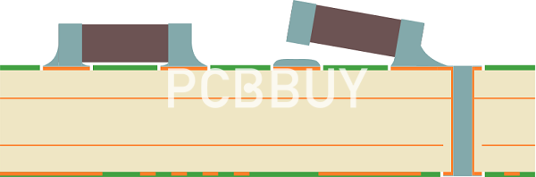
The tombstone defect in PCBs refers to the partial or complete lifting of passive SMT (surface-mount technology) components from the PCB pad. While one end gets soldered on the chip, the other stands up. Visually, it gives the appearance of a tombstone.
The tombstone defect is also called the Manhattan effect, Stonehenge effect, or Drawbridge effect. Tombstoning PCBs aren’t limited to passive devices. It can also occur on a surface mount device and can be a fatal defect.
2. What causes the tombstone effect?
The usual suspects for the tombstone effect are:
· Lack of thermal balance - one pad melts before the other.
· Insufficient solder dam - solder flows from a surface-mount pad into a nearby hole
· Uneven application of solder paste - different surface tension on each pad
· Placement offset - part not correctly centered during pick and place
3. What is the performance of Tombstone PCB?
As the name suggests, tombstoning resembles those large, sometimes slanted slabs of granite that you’ll find at a cemetery. In the case of a PCB design, tombstoning is typically a surface mount passive component, like a resistor or a capacitor, that partially lifts from a pad on one end. As your component stands on end like it’s rising from the dead, it ends up looking like a tombstone in the graveyard of what is now a defunct PCB design with an open circuit.
While the angle of a lifted tombstone component can vary, it all means the same thing. There’s going to be some post-soldering rework done by your manufacturer, and you’ll likely be sending more money their way to correct the issue. In the early days of PCB manufacturing, tombstoning was an issue related to the process of vapor phase reflow technologies. But as these vapor technologies declined in use, manufacturers and designers assumed that tombstoning issues would cease to exist. But they were wrong.

4. What are the causes of Tombstone PCB?
Take a simple SMD resistor as an example, which has two pads. In an ideal process, the solder will attach itself to both pads and complete its wetting process at the same time on both ends. No tombstoning issues here. But you run into a problem when the wetting process of solder is unbalanced. Like when the solder on one pad completes its wetting process before the other, which results in one side of a component solidifying while the other is still in process, and so begins the game of tug-o-war.
Of course, the wet pad ends up winning, pulling up the other pin still in the process of wetting, and the entire component gets tilted on its side, looking like a tombstone. As you can imagine, identifying exactly what caused this uneven wetting can be quite the detective work as there are so many variables in play during a typical wave reflow process. Some of the most common causes of a tombstoning issue on a PCB can include:
· The temperature of the reflow oven being uneven, which can cause the solder to begin and finalize its wetting process at different times on your PCB layout.
· Solder paste being applied to your board in a non-uniform application across all of your pads which can lead to wetting beginning and ending at different times.
· There’s also the varying sizes of pads themselves, with SMT pads having their own set of tolerances that are often ignored but can affect the accuracy of solder applications.
5. What are the effective methods of preventing Tombstone PCB?
There are three main DFM areas to focus on that will help you to prevent tombstoning from occurring on your PCB design:

Footprint pad size: If the pad sizes for your small passive parts are incorrect, it could affect the thermal mass of the solder joints. A pad with less mass will cause the solder to reflow sooner than larger pads. It is important, therefore, to follow industry standards or the manufacturer’s recommended sizes when you build the CAD footprint pads.
Footprint construction: Along with building the pads to the correct size, you also need to ensure the entire footprint for the passive parts is built correctly. If the part is not centered on its origin, it could lead to problems as you saw in the video. You also must ensure that the pads are correctly spaced and that you are using the same size pad for both pins of the part. Again, the key is to follow industry standards and the manufacturer’s recommendations when building your footprints.
Trace routing and power planes: Even if you have a perfectly sized and balanced CAD footprint, there could still be a risk of differing thermal mass between the pads if the routing is not balanced. Connecting one pad with a thin trace while connecting the other pad with a thick trace will create an imbalance in the thermal mass of the two pads. The additional metal will act as a heat sink, causing the solder paste on that pad to melt slower than the other. Embedding a pad within a power plane is even worse, as the larger area of metal will pull more heat with it. Be careful to balance the routing between the two pads as much as possible, and use thermal ties when connecting a pad directly to a metal plane.
By following these recommendations, you have a much better chance of avoiding tombstoning of your small passive parts. Here’s another way that you can get some help with your design so that it will be more easily manufactured.
Industry Category


