What Are the Applications of Multilayer PCB?
By:PCBBUY 08/30/2024 17:24
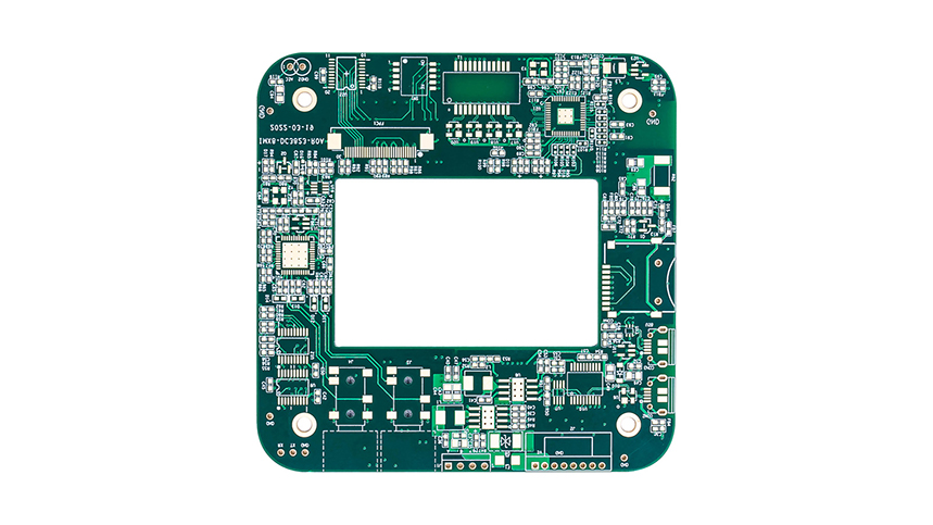
Multilayer Printed Circuit Boards (PCBs) are integral to the design and functionality of modern electronics. Comprising three or more conductive layers stacked with insulating layers in between, multilayer PCBs offer enhanced electrical properties, increased reliability, and improved signal integrity compared to single-layer and double-layer boards. This article explores the various applications of multilayer PCBs, focusing on the technical advantages they offer, industry-specific uses, and the role they play in advancing technology.
1. Understanding Multilayer PCBs
1.1 What is a Multilayer PCB?
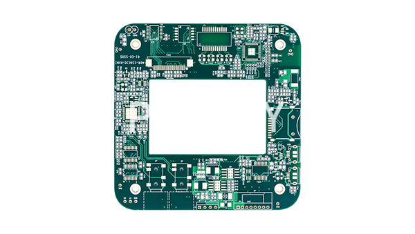
Multilayer PCBs consist of multiple layers of circuitry stacked on top of one another, separated by insulating material, also known as the dielectric. These layers are interconnected using vias (plated holes) to form a cohesive and complex electronic circuit. Typical multilayer PCBs can range from 4 to 40 layers, depending on the complexity of the design and the requirements of the application.
-
Definition: A PCB with three or more conductive layers, which are separated by dielectric materials and interconnected through vias.
-
Structure: Alternating layers of conductive copper and insulating dielectric material, all compressed together.
1.2 Advantages of Multilayer PCBs
-
Increased Component Density: The ability to stack layers allows for a higher density of components, which is essential in compact devices.
-
Improved Signal Integrity: Multilayer designs can reduce electromagnetic interference (EMI) and crosstalk, providing cleaner signal transmission.
-
Enhanced Performance: Multilayer PCBs can support high-speed signals and high-frequency operations, making them suitable for advanced computing and communication systems.
-
Reduced Size and Weight: By consolidating circuitry into multiple layers, the overall size and weight of the device can be reduced, which is crucial in portable and wearable technology.
2. Applications of Multilayer PCBs in Various Industries
Multilayer PCBs find applications across a broad range of industries, each benefiting from their unique properties.
2.1 Consumer Electronics
The consumer electronics market heavily relies on multilayer PCBs due to the need for compact, high-performance devices.
-
Smartphones and Tablets: Multilayer PCBs are crucial in smartphones and tablets, where space is limited but high performance is required. These devices typically use 8-12 layer PCBs to accommodate processors, memory chips, and communication modules.
-
Wearable Devices: Smartwatches and fitness trackers use multilayer PCBs to integrate sensors, communication chips, and processors in a compact form factor. The typical PCB thickness in these devices is less than 1mm to maintain comfort and usability.
-
Home Appliances: Modern home appliances such as smart refrigerators, washing machines, and ovens utilize multilayer PCBs to manage complex functions, connectivity, and smart features.
2.2 Telecommunications
The telecommunications industry demands high-speed data transmission and minimal signal loss, making multilayer PCBs ideal.
-
Routers and Switches: Multilayer PCBs support the high-speed data processing requirements of routers and network switches. These devices often use 12-24 layer PCBs to manage data traffic efficiently.
-
Base Stations: Cellular base stations require robust and reliable PCBs to handle high-frequency signals. Multilayer PCBs help in reducing interference and enhancing signal clarity, which is critical for mobile communication.
-
Satellite Communication: In satellite systems, weight and reliability are key factors. Multilayer PCBs provide a lightweight solution with high reliability, suitable for space applications where maintenance is challenging.
2.3 Automotive Industry
The automotive industry increasingly integrates electronic components for various functions, from entertainment to safety.
-
Infotainment Systems: Modern cars are equipped with infotainment systems that provide navigation, entertainment, and connectivity. These systems rely on multilayer PCBs to handle multiple functions simultaneously without interference.
-
Advanced Driver Assistance Systems (ADAS): Safety features such as lane departure warning, collision detection, and adaptive cruise control use multilayer PCBs to process data from various sensors and make real-time decisions.
-
Electric and Hybrid Vehicles: Power management and battery control systems in electric and hybrid vehicles use multilayer PCBs to ensure efficient power distribution and energy management. These PCBs need to withstand high temperatures and provide reliable performance.
2.4 Medical Devices
Medical devices demand high precision, reliability, and compact design, making multilayer PCBs an ideal choice.
-
Diagnostic Equipment: MRI machines, CT scanners, and ultrasound devices require multilayer PCBs for signal processing and control functions. The boards ensure accurate data collection and transmission with minimal noise.
-
Implantable Devices: Pacemakers and neurostimulators use miniature multilayer PCBs to achieve the required functionality within a small, implantable form factor. These PCBs must meet strict reliability and biocompatibility standards.
-
Portable Medical Devices: Devices like blood glucose monitors, portable ECG machines, and hearing aids use multilayer PCBs to integrate complex circuitry in a compact, portable form factor.
2.5 Aerospace and Defense
The aerospace and defense industries require durable and reliable electronics that can operate under extreme conditions.
-
Avionics: Aircraft control systems, navigation, and communication devices use multilayer PCBs to handle the high-speed data processing and ensure reliable operation in harsh environments.
-
Military Communication Systems: Secure and reliable communication is critical in military operations. Multilayer PCBs provide the necessary signal integrity and EMI protection for secure communication devices.
-
Guidance and Control Systems: Missiles and unmanned aerial vehicles (UAVs) use multilayer PCBs for precise control and navigation, requiring high reliability and performance.
3. Design Considerations for Multilayer PCBs
Designing multilayer PCBs requires careful consideration to meet the application's specific requirements.
3.1 Layer Stack-Up Design
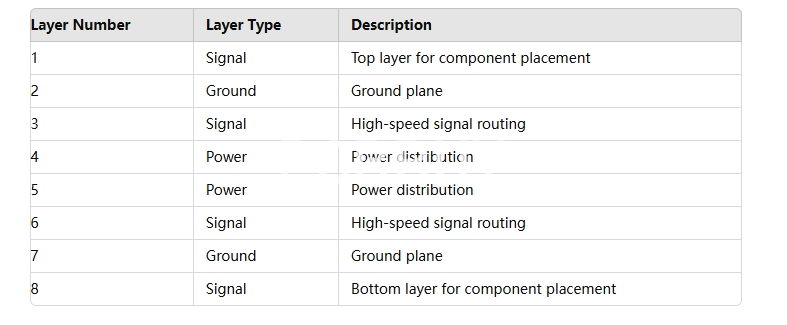
Layer stack-up is the arrangement of the conductive and insulating layers in a PCB. A well-designed stack-up minimizes EMI, supports impedance control, and ensures thermal management.
-
Example Stack-Up: A typical 8-layer PCB may include power planes, ground planes, and signal layers, arranged to minimize interference and provide effective heat dissipation.
3.2 Via Design
Vias are essential for connecting different layers in a multilayer PCB. Choosing the correct via type is critical for reliability and performance.
-
Types of Vias:
-
Through-Hole Vias: Penetrate all layers and are used for general connections.
-
Blind Vias: Connect outer layers to one or more inner layers but do not pass through the entire board.
-
Buried Vias: Connect only internal layers and are not visible on the board surface.
3.3 Signal Integrity and Impedance Control
Maintaining signal integrity is crucial in high-speed and high-frequency applications.
-
Differential Pair Routing: Used for high-speed signals to reduce noise and crosstalk.
-
Controlled Impedance: Maintaining consistent impedance through careful trace width and spacing ensures signal quality. The impedance can be calculated using the formula:

4. Challenges in Multilayer PCB Manufacturing
While multilayer PCBs offer many advantages, they also present several challenges during manufacturing.
4.1 Registration Accuracy
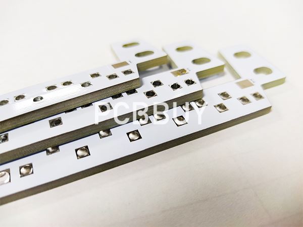
Accurate alignment of layers is critical to ensure that vias connect correctly and that signal traces are aligned. Misalignment can cause shorts, open circuits, or signal integrity issues.
4.2 Delamination
Delamination occurs when layers separate, usually due to poor lamination processes or thermal stress. It can lead to reduced reliability and board failure.
4.3 Cost Considerations
Multilayer PCBs are more expensive to manufacture than single or double-layer PCBs due to the complexity of the process and the materials used. Costs can be managed by optimizing the layer count and using cost-effective materials without compromising performance.
5. Future Trends in Multilayer PCB Technology
As technology advances, multilayer PCBs continue to evolve to meet new challenges.
5.1 Increased Layer Count
The demand for higher performance and more functionality drives the need for PCBs with 30 or more layers. These boards are used in advanced computing, telecommunications, and defense applications.
5.2 Integration with Flexible and Rigid-Flex PCBs
Combining rigid and flexible PCBs allows for more complex designs that can bend and fold, making them suitable for compact and dynamic applications, such as foldable smartphones and wearable devices.
5.3 Use of Advanced Materials
New materials with better electrical and thermal properties are being developed to support high-frequency applications, such as 5G technology and high-speed computing.
Conclusion
Multilayer PCBs play a vital role in the advancement of modern electronics, offering compact size, high performance, and reliability. Their applications span across industries, from consumer electronics and telecommunications to automotive, medical, aerospace, and defense. By understanding the design considerations and challenges associated with multilayer PCBs, engineers can harness their full potential to create innovative and efficient electronic devices.
References
-
IPC-2221, “Generic Standard on Printed Board Design,” IPC, 2020.
-
Johnson, H. W., & Graham, M., “High-Speed Digital Design: A Handbook of Black Magic,” Prentice Hall, 1993.
-
Miller, W., “Design for Manufacturability: Multilayer Printed Circuit Boards,” Circuits Assembly Magazine, 2018.
-
Rogers Corporation, “High-Frequency Circuit Materials,” Rogers Corporation, 2021.
-
Weller, R. M., “Advanced Multilayer PCB Design: A Comprehensive Guide,” PCB Design Magazine, 2019.
Industry Category


