What Are the Applications of Multilayer PCB?
By:PCBBUY 11/06/2023 14:30

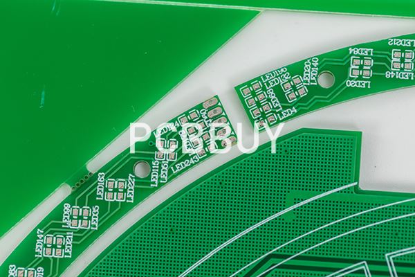
Multilayer PCB is a Printed Circuit Board with more than 2 layers. A Double-Sided PCB has two conductive layers on top and bottom of the PCB substrate. A Multilayer PCB must have a minimum of 3 conductive layers of conductive material or copper layer. All the layers are interconnected with copper plated holes. The layers can be 4, 6, 8…upto 40 layers.
A multilayer PCB is complex by design. The top and bottom layers look same as a double sided PCB but has staked layers on both sides of the core. All the layers are compressed to form a single Multilayer PCB where all the layers are interconnected via copper plated holes.
How to make multilayer PCB? If you are a beginner of PCB industry, please check and read the content below in this passage for more professional knowledge.
What Are the Applications of Multilayer PCB?
Consumer Electronics
The term “Consumer Electronics” is a wide term that includes many electronic devices that comes under the umbrella of commonly used devices that are directly relevant to common users like you and me. The consumer electronics include, smartphones, smart watches, calculators, TV remote control, mp3 music player, toys, kitchen appliances, washing machines, electric kettle, e-cigarettes, LED bulbs and energy savers etc.
Computers and Devices
Today our world is highly dependent on computers and automation. Multilayer PCBs are commonly found in computers and associated products like motherboards, graphics cards, EEPROMs, Power supplies, keyboard, computer mouse, ADCs, GPUs, Image processing circuits etc.

How to identify multilayer PCB?
When calculating the needs of a printed circuit board, consider the types of machines and devices your PCBs will be used in and the demands these machines/devices will place on the board circuitry. Will these PCBs be used in high-tech, complex electronics or in simpler items with minimal functions? Other things to consider are the manufacturing costs of single- and double-layer PCBs versus multilayer. If you want to have the highest capacity possible in today's circuit board technology, you will need to pay for the high manufacturing costs involved.
Lead time - the time it takes to manufacture a set of PCBs of single vs. multiple layers - is also something to consider when you order a large shipment of printed circuit boards. The lead time for one- and two-layer boards could be anywhere from 8 to 14 days, depending on the size of the board area. Then again, if you are willing to pay more or less, the lead time could be as short as five days or as long as a month. The lead time will increase, per board size, with every layer you add to the order. PCBs in the four- to 20-layer range could have a lead time of anywhere from 12 to 32 days, depending on whether you want the boards to have small or large dimensions.

How to build multilayer PCB stackup?
Step 1: Inner layer core selection
The stack-up designates the materials to be used for the manufacture of a multilayer circuit board. The build-up provides the following information:
·The copper thickness and weight
·Type of epoxy glass to be used
·Panel size
Step 2: Cleaning
The inner layers are cleaned chemically/mechanically or both to remove contaminants from the copper surface.
Step 3: Inner layer imaging
The imaging material is placed on the copper surface. It covers the desired copper circuitry and exposes the unwanted copper.
Step 4: Etch stripping
The inner layers are chemically etched to get rid of the unwanted copper. The photoresist is then stripped off to reveal the copper circuitry.
Step 5: Automated Optical Inspection
Automated optical inspection is carried out to find the flaws(shorts/opens in inner layers) that can’t be detected by the human eye.
Step 6: Oxide treatment
The exposed copper circuitry on the inner layer must be treated before lamination to improve adhesion. Improved adhesion also increases the structural strength and overall board reliability.
Step 7: Layup
Steps 1 to 6 are repeated for all the inner layers. For example, these steps will be carried for layers 2, 3, and 4, 5.
Industry Category


