What Are the Basic Guidelines of PCB Footprint Design?
By: PCBBUY 09/23/2024 15:04
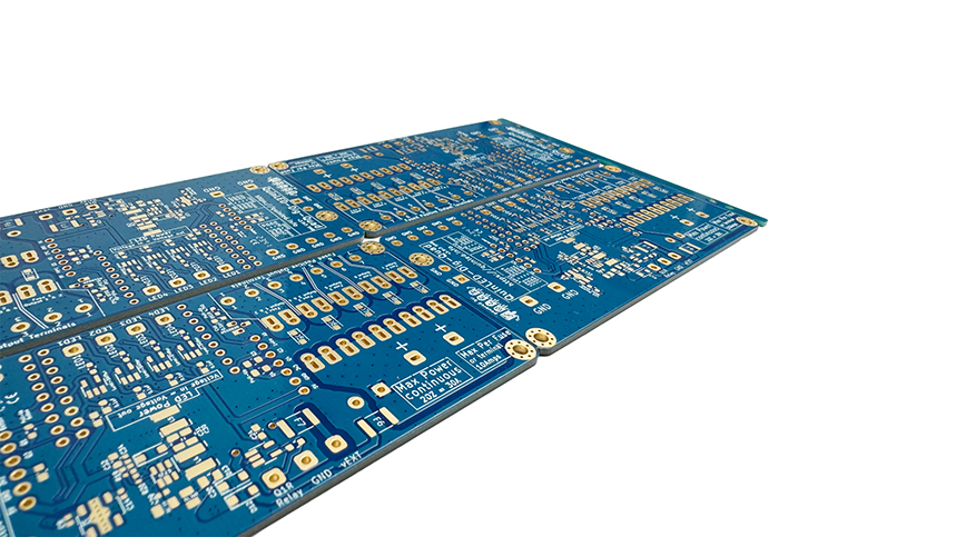
Printed Circuit Board (PCB) footprint design is critical to ensure the reliable assembly and functionality of electronic components. A well-designed footprint not only ensures that the component will fit the board physically, but also enhances the electrical performance and ensures proper manufacturing. This article will cover the basic guidelines for PCB footprint design, providing technical insights into its principles, standards, and how each element of the footprint affects the overall PCB performance.
1. Introduction
A PCB footprint is the physical layout pattern on the PCB where a specific electronic component will be mounted. It includes the arrangement of copper pads, solder mask layers, silkscreen layers, and other critical features that ensure the proper mechanical and electrical connection of the component. Effective PCB footprint design is fundamental in creating a manufacturable, reliable, and high-performance PCB.
2. Importance of PCB Footprint Design
The footprint of a PCB is the foundation upon which the entire electronic assembly is built. A poorly designed footprint can lead to assembly issues, such as misaligned components, short circuits, or open circuits. It can also negatively affect the electrical performance by increasing resistance or affecting impedance control. As PCBs become smaller and more complex, footprint design becomes even more critical, requiring designers to follow strict guidelines and standards.
3. Essential Components of a PCB Footprint
3.1 Pad Design
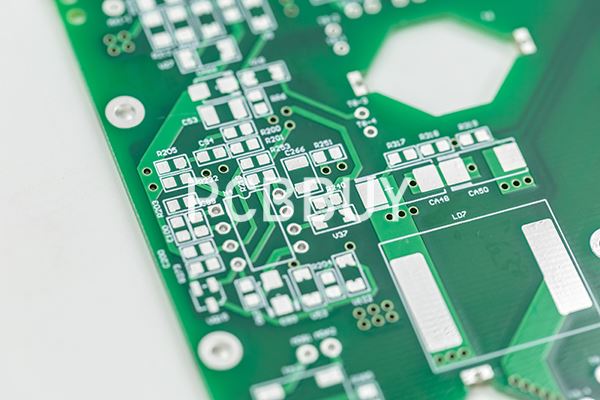
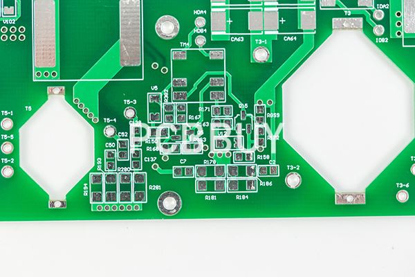
Pads are conductive areas where component leads or pins are soldered to the PCB. They are typically made of copper and may be coated with other metals to improve solderability. Pads can be through-hole or surface mount, and their size and shape must match the component’s leads to ensure a good solder joint.
Through-hole pads: These are used for components with leads that pass through the PCB. They are typically larger and require a hole to be drilled in the PCB.
Surface-mount pads: These pads are for components mounted on the surface of the PCB. The size of the pad depends on the component’s lead or ball grid array (BGA) size.
3.2 Silkscreen and Placement Outline
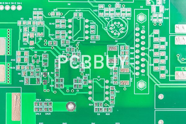
The silkscreen layer provides visual cues for the placement and orientation of components. It usually includes reference designators and polarity markings for components like diodes or capacitors. The placement outline helps guide accurate component positioning during assembly.
3.3 Courtyard Area
The courtyard area defines the boundary around a component where no other components or pads should be placed. This ensures enough space for assembly and inspection, preventing short circuits and solder bridging.
3.4 Thermal Relief Pads
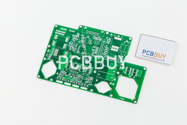
Thermal relief pads are designed to help heat flow during soldering, ensuring that components are soldered properly without overheating the entire PCB. They are especially important for components with large copper planes, like power transistors or connectors.
4. Design Standards for PCB Footprints
4.1 IPC-7351 Standard
The IPC-7351 is the most commonly used standard for PCB footprint design. It provides rules for the size, shape, and spacing of pads and other features, helping to ensure manufacturability and reliability.
4.2 JEDEC Standard
JEDEC standards are primarily used for semiconductor devices and define dimensions, pin configurations, and footprint requirements for integrated circuits (ICs) and other components.
5. Electrical Considerations
5.1 Impedance Matching
In high-speed designs, impedance matching is critical to prevent signal reflection and degradation. The width of the traces and the spacing between the pads influence the impedance of the circuit. Controlled impedance can be calculated using the following formula:

5.2 Trace Width and Pad Spacing
The trace width must be designed to handle the required current without causing excessive heat or voltage drop. Pad spacing must also be carefully designed to prevent electrical shorting, particularly in high-voltage applications.
6. Manufacturing Considerations
6.1 Component Placement Accuracy
Proper placement of components during assembly is crucial for soldering and the overall performance of the PCB. Incorrectly placed components may not align with the pads, leading to weak or faulty solder joints.
6.2 Surface Mount Technology (SMT) and Through-Hole Technology
Different assembly processes require different footprint designs. SMT components require smaller, precise pads, while through-hole components need drilled holes and pads on both sides of the PCB.
7. Chemical Reactions in PCB Manufacturing
7.1 Copper Plating and Etching Process
Copper etching is a critical process where unwanted copper is removed from the PCB, leaving behind the desired circuit traces. The chemical reaction for copper etching using ferric chloride is:
2FeCl3 + Cu → 2FeCl2 + CuCl2
This reaction removes the copper layer, forming copper chloride and ferric chloride.
7.2 Solder Paste and Reflow
Solder paste is applied to the pads, and during reflow, it melts and solidifies to create a strong connection between the component leads and the pads. The key chemical component in solder is typically a tin-lead alloy (Sn-Pb), though lead-free solders are becoming more common, such as tin-silver-copper (SnAgCu).
8. Advanced Techniques for High-Density Designs
8.1 Via-In-Pad and Microvias
As PCBs become denser, designers often use via-in-pad technology, where the via is placed directly in the pad to save space. Microvias are also used to connect different layers of the PCB in a smaller footprint.
8.2 Blind and Buried Vias
Blind vias connect an outer layer to an inner layer, while buried vias connect two inner layers without appearing on the outer surfaces. These techniques help save space in multi-layer PCBs.
9. Best Practices for Reliable Footprint Design
9.1 Clearance and Tolerances
Clearance between pads, traces, and components must adhere to the minimum requirements set by the manufacturer. Tolerances ensure that variations during manufacturing don’t lead to faults.
9.2 Component Orientation and Rotation
Components should be placed in a consistent orientation to aid in assembly and testing. Proper rotation also ensures the correct electrical connections are made.
10. Common Errors in PCB Footprint Design
Some common errors include:
- Incorrect pad sizes, leading to weak solder joints.
- Inadequate clearance between components, leading to short circuits.
- Misaligned silkscreen, causing confusion during assembly.
Conclusion
PCB footprint design is a crucial step in ensuring the manufacturability and reliability of a PCB. By following established guidelines and standards, designers can avoid common pitfalls and ensure that their designs are ready for assembly and operation. With the increasing complexity of electronic devices, careful attention to footprint design will continue to be a fundamental aspect of PCB development.
References
1. IPC-7351 Standard for Surface Mount Design and Land Pattern Standard.
2. JEDEC Standard JESD30E: Requirements for Soldering and Land Pattern Design.
3. Ulrich, R. K., & Schaper, L. A. (2003). Fundamentals of Electronic Circuit Board Design.
4. Ritter, J. J. (2018). Designing for High-Density PCBs.
Industry Category


