What Are the Characteristics Uses and Classifications of HDI/BUM PCB?
By:PCBBUY 07/03/2024 17:49
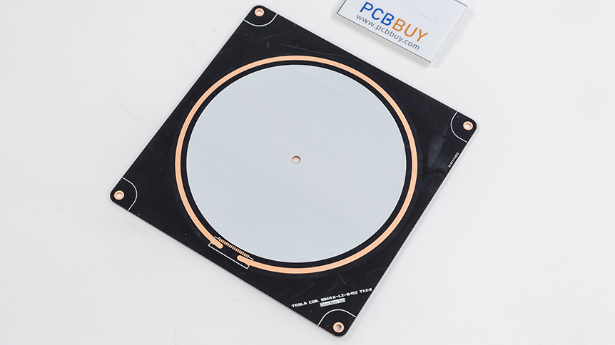
The build-up multilayer PCB (BUM) refers to a multilayer printed circuit board formed by coating an insulating medium on an insulating substrate or traditional printed circuit board, then using chemical copper plating and electroplating processes to form circuits and connection holes, and finally stacking multiple layers to achieve the desired number of layers. This concept was initially proposed by the Japanese and later adopted in the West as high-density interconnection technology (HDI). Literature on BUM technology dates back to 1976, and in 1991, IBM (Japan) developed a new technology for coating photoresist on the core board to form conductive microvias through photolithography, using an additive method for circuit formation. By 1999, mass production had been achieved, and since the 21st century, it has been widely used in portable electronic products such as laptops, mobile phones, digital cameras, and MCM packaging substrates.
This technology can produce thin, multilayer, stable, high-density interconnection printed circuit boards that conventional multilayer board technology cannot achieve. It meets the demands of electronic products evolving towards lighter, smaller, thinner, and more reliable devices, satisfying the needs of new-generation electronic packaging technology with increasing packaging density.
Characteristics, Uses, and Classification of HDI/BUM Printed Circuit Boards
Characteristics of HDI Boards
HDI boards stand out due to their high-density design, featuring five main characteristics compared to traditional printed circuit boards:
1. Incorporation of Blind Vias: These are generally created using laser drilling rather than mechanical drilling, as current drilling techniques can produce 0.15mm mechanical drill bits, but these require high rotational speeds and slow vertical drilling speeds to prevent breakage. Despite advancements, the drill breakage rate remains high, and special parameters reduce drilling efficiency, making laser drilling preferable for HDI boards.
2. Small Via Sizes: Vias typically have a diameter below 150μm with pad sizes below 250μm. Reducing via size and pad dimensions increases available space for other components, enhancing functionality within a fixed or reduced footprint.
3. High Solder Joint Density: Exceeding 130 points/in², the increased density allows for more components and functionality.
4. High Routing Density: Exceeding 117 in/in², increased routing density is essential for accommodating more components.
5. Narrow Line Widths and Spacings: Lines and spaces not exceeding 3 mil. Although the strict definition of HDI requires 75μm/75μm, a more common specification is 100μm/100μm due to manufacturing capabilities and cost considerations.
What Are Uses of HDI Boards?
HDI technology has become a predominant circuit board manufacturing technology, significantly contributing to markets such as 4G smartphones, advanced digital cameras, and IC substrates in mobile communications. Data shows that from 2000 to 2008, the global growth rate of HDI printed boards exceeded 14%, far outpacing other types of circuit boards. This indicates the promising future of HDI technology in the printed circuit board field.
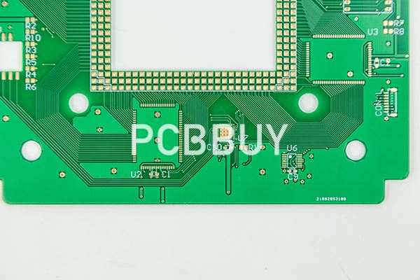
HDI boards, due to their light weight, thin layers, short transmission paths, high wiring density, small volume, low noise, high reliability, wide application range, and multifunctionality, are widely used in electronic communication and mobile devices.
In summary, HDI boards possess "Four Highs and One Low": high wiring density, high frequency and speed, high connectivity, high insulation reliability, and low cost.
What Are the Classification of HDI Boards?
HDI boards can be classified into three common types based on the characteristics of blind vias and the number of build-up layers:
1. 1+N+1 Type: High-density interconnection printed circuit boards formed by a single build-up process.
2. i+N+i (i≥2) Type: High-density interconnection printed circuit boards formed by two or more build-up processes, with different layers of microvias either staggered or stacked. Electroplated filled stacked microvia structures are common in high-demand designs.
3. Full Layer Interconnection Type: All layers are high-density interconnection layers, allowing free interconnection of conductors through stacked electroplated filled microvias. This structure provides reliable interconnection solutions for complex large pin-count devices like CPUs and GPUs used in handheld and mobile devices.
What Are Material Performance Requirements for HDI/BUM PCB?
Materials used in HDI printed circuit boards product have evolved to meet the "Four Highs and One Low" requirements, advancing at different stages of HDI development and substrate material technology levels. The core content remains the same: materials must meet the high-density development needs of printed circuit boards, such as better anti-electrostatic migration and dimensional stability.
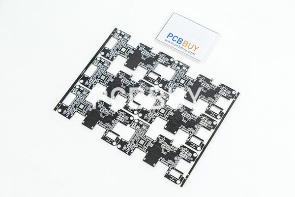
Based on basic characteristics, application processability, cost, and other factors, the following materials are expected to dominate the future market:
1. Prepreg (PP) Materials: Comprising resin and reinforcing materials (mostly fiberglass for multilayer circuit boards), these materials enhance the mechanical and thermal stability of the dielectric layer. PP materials have a low cost but slightly weaker reliability compared to other materials, making them suitable for low-end, high-consumption electronic consumer products like mid- to low-end mobile phones.
2. Resin Coated Copper (RCC) Materials: Available in three types—PI metallized film, PI film with adhesive, and cast PI film—RCC materials offer good processability and high product reliability, with strong peel strength for surface pads, making them suitable for high-demand drop tests.
3. Laser Drillable Prepreg (LDP) Materials: These materials are cost-effective compared to RCC, with reliability superior to PP materials. They are widely used in HDI printed boards for high-end mobile phones and electronic products, providing strong rigidity and excellent anti-peel strength.
4. Liquid Crystalline Polymer (LCP) Materials: LCP, a thermoplastic insulating resin developed by Japan's Mektron for high-frequency multilayer printed boards, boasts excellent high-frequency characteristics, dimensional stability, and environmental friendliness. It is gradually replacing traditional PCB materials like PI due to its superior processing and physical properties.
What Is Manufacturing Process Technology of HDI/BUMPCB with Core Boards?
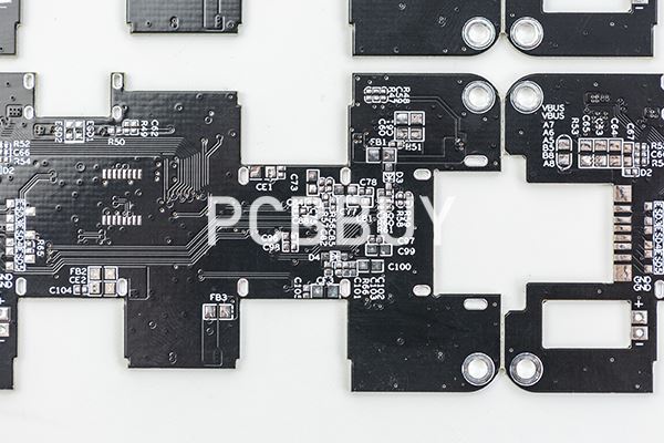
The manufacturing process technology of HDI printed circuit boards, encompassing material, structural, and technological innovations, is crucial. Most build-up multilayer printed circuit boards are manufactured using core boards, with n layers (usually n=2-4) built up on the conventional board's single or double sides, forming a high-density printed circuit board. The single or double-sided printed circuit boards used for building up are called core boards of build-up multilayer printed circuit boards.
What Is Conductive Hole Plugging Technology for HDI/BUM PCB with Core Boards?
Plugging conductive holes in the core board mainly provides a high flatness surface for the build-up layers. As these layers may be "built" on the core board's conductive holes, the core board's conductive holes must undergo a plugging process. This process can use either insulating or conductive materials.
1.Insulating Plugging Materials
These materials, such as thermosetting epoxy or liquid solder mask, fill the conductive holes after metallization, offering a flat surface and preventing impurities from entering the holes, thus aiding lamination or vacuum pressing. However, these materials can shrink significantly during curing or degassing, potentially leading to mechanical failures.
2. Conductive Plugging Materials
Composed of polymer binders and conductive particles (e.g., silver or copper), these materials provide a flat surface and enhance electrical and thermal conductivity. Conductive plugging materials must have minimal shrinkage to prevent delamination and barrel cracking. Materials like DuPont's silver/copper/epoxy paste, which can fill holes with a 6:1 aspect ratio, are ideal. These materials should also withstand high electrical and thermal stress and have minimal shrinkage to ensure reliable hole plugging.
By translating the document into English, the comprehensive overview of HDI/BUM printed circuit boards, including their characteristics, applications, classifications, material performance requirements, and manufacturing process technologies, is preserved. This detailed information can serve as a valuable resource for professionals and researchers in the field of electronics and printed circuit board manufacturing.
Typical properties of DuPont's silver/copper/epoxy conductive adhesive
|
Condition measurement item |
Typical result |
|
Volume resistivity |
0.000162 cm |
|
Plugging via resistance (hole size 0.33 mm, board thickness 0.64 mm) |
<10mQ/ Plugging |
|
Thermal conductivity |
> 5.2 w/(m K) |
|
Linear CTE |
<35ppm/C |
|
Thermal cycle (-65C ~ 125C) |
No degradation after 1000 times |
|
Thermal stress (10s in Sn/Pd at 288C) |
Impregnation 5 times without degradation |
|
Adhesive force of paste |
7 to 10 pounds on BT and FR-4 |
|
Electroplatability (copper) |
Electroplating and electroless copper plating are available |
Conductive Hole Filling and Core Board Processing in HDI PCBs
Electroplating can also be used to fill via holes and close them, but this method has the following issues: firstly, it requires a long plating time, resulting in low production efficiency and high costs; secondly, there is a risk of entrapping corrosive electroplating solutions inside the via holes, posing a potential reliability threat; thirdly, the thick copper layer on the board surface is unfavorable for the fabrication of fine lines and soldering.
3. Filling of Via Holes
After drilling, metallization, and electroplating of the core board in an HDI board, the via holes must be filled with conductive paste or other materials to ensure their performance requirements. The filling of via holes is mostly achieved through stencil printing. The stencil is usually made based on the size and shape of the via holes, using stainless steel sheets. The required mesh size and shape are then formed using laser and photo-etching methods, and a squeegee is used to press the conductive paste through the mesh into the via holes.
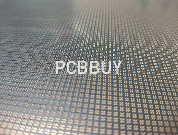
For core boards with a thickness-to-diameter ratio less than 3:1, one or two passes of stencil printing with a squeegee can easily fill the via holes. For core boards with higher thickness-to-diameter ratios, a vacuum table should be used. This vacuum table printing technology has been applied in the processes of silver paste and carbon paste filling for small holes.
4. Flattening (Board Scrubbing)
After the via holes on the core board are filled through printing, they must be dried for further processing. Conductive paste always contains a certain amount of solvent or dispersant to facilitate printing and pressing into the via holes, which should be evaporated during drying. Currently, conveyor-type infrared drying systems are widely used, significantly improving drying efficiency and productivity, with drying times typically around 15-30 minutes at approximately 115°C. To remove the contamination (especially resin parts) on the board surface during printing and the raised parts due to stencil thickness and lifting, the drying temperature should not be too high to avoid curing difficulties and making it hard to brush off.
After drying, the core board is processed using conventional board scrubbers equipped with abrasive disks (made of alumina or pumice powder) or brush rollers (nylon brushes containing alumina) to remove surface contaminants and protruding conductive paste, achieving a smooth and clean surface.
The flattened core board then undergoes curing to ensure that the resin in the conductive paste fully cross-links, thereby firmly bonding the conductive particles to the copper foil inside the via holes. The curing temperature should be above the resin's Tg (glass transition temperature). For epoxy systems, the curing temperature is approximately 160°C for about 60 minutes. During curing, the resin forms a network structure, increasing in density and potentially causing shrinkage. However, since metal particles in the conductive paste typically account for more than 95% by weight, and the thermal expansion coefficient (CTE) of the resin is less than 35 ppm/°C, this shrinkage can be effectively managed to match the CTE of the core board.
Reference
He Wei, PCB Basic Electrical Information Science and Technology, China Machine Press,328-334
Industry Category


