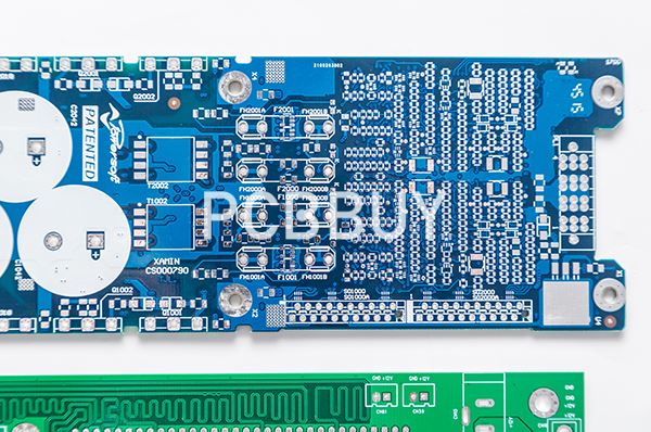
What Are the Common Defects of PCB Soldering?
By:PCBBUY 03/14/2024 16:38

As smart phones, tablets, and wearable devices have become smaller, thinner, and more functional, PCBs and components continue to be even smaller, denser, and more layered. In the automotive industry, research and development of technologies such as automatic brakes and autonomous driving has promoted computerized control of important components.
To evaluate the durability and reliability of PCBs and electronic components, reliability evaluation tests, including acceleration tests, have become increasingly important. In addition to such tests, using microscopes to identify defects and failure causes is more important than ever. If you are searching for more information about PCB assembly defects, please check and read the content below.
What Are the Common Defects of PCB Soldering?
Soldering defects can arise for a variety of reasons, ranging from operator error to pollutants. The most well-known -- and well-hated -- of these defects are:
· Opens
· Excessive solder
· Component shifting
· Cold joints
· Solder bridges
· Webbing and splashes
· Lifted pads
As frustrating as these defects can be, it’s a valuable lesson to experience them at least once. And, to pass the solderability test standard, knowledge of soldering defects is critical.
Pin and Connector Checks
One of the important components of PCB is the pin and connector, which help relay signals in operations. Incorrect placement of the pin can result in damage to the connector. To prevent this defect, you can use a pattern-matching tool to check the connector’s correct placement.
Thus, you can use this pattern-matching tool, usually in a vision tool kit, to locate and group patterns. Hence, it provides a score that indicates how much the patterns match the intended pattern or location.
However, to ensure the alignment of pins, you can use a telecentric lens. The magnification of a telecentric lens does not change, which prevents parallax error, which a conventional lens can cause. However, a thorough check of pins and connectors will go a long way in preventing this defect in cheap correct PCB service provider. Thankfully, there are various PCB manufacturing companies.

Heat Dissipation Analysis
Most electronic components tend to get unusually hot whenever they are working at their full capacity. Hence, this can lead to overheating if they are not properly checked. Also, a hot PCB heat sink can be a shock to unsuspecting technicians. Likewise, PCB’s extreme temperatures can lead to a reduced lifespan of products hence. Leading to a waste of money and the poor reputation of manufacturing companies.
Thus, to protect your PCB design from overheating. You will have to solder an SMD heat sink, which usually has a thermal pad against a heat spreading pattern on the PCB. Also, an SMD heat sink is then soldered on the end of the copper, which will promote better dissipation of heat. Furthermore, you must ensure that the safety limit is not exceeded. The heat sink is not overly hot, such that it can damage the skin.
By using an SMD heat sink, however, heat will dissipate in proper measures in high power components. Thus, ensure that you use the SMD heat sink’s right size or shape when soldering it onto the PCB.
BOM problems:
Bill of materials that contain incorrect data can cause the wrong parts to be ordered and installed on the board. Additionally, BOMs can collect outdated information and specify parts that are not available for manufacturing. Before a circuit board is sent out for manufacturing, review its BOM for the following:
Correct parts
Part numbers that match their descriptions
PCB footprints that are correctly associated with their parts
Parts that may not be available due to being obsolete (OBS), recommended for new designs (NRND), or end of life (EOL)

Incorrect PCB footprints
As we just stated, it is imperative to check the BOM to make sure that the right footprint is associated with the part. A review of the PCB footprints shouldn’t stop with just the BOM, though. Check that the footprint is built correctly according to industry standards and the manufacturer’s datasheet. This scrutiny should also include the footprint pads to ensure that the part will sit down and solder correctly to the circuit board.
DFM errors
Design for manufacturability is one of the most vital criteria for designing a circuit board. Ensure that the components are placed with correct spacing to each other and the edge of the board or other mechanical board objects. Without this spacing, the parts may not be assembled using automated equipment, which will add a lot of time and cost to the manufacturing of the board.
Industry Category


