What Are the Common PCB Manufacturing Challenges?
By:PCBBUY 03/06/2024 15:18

Electronics and PCB manufacturing is presently facing several challenges together with opportunities. Along with the need to control costs, the PCB manufacturing services will have to focus on finding ways of capitalizing on current trends.
If you are going to learn more about fast turnaround PCB prototype, please check and read the content below for more information.
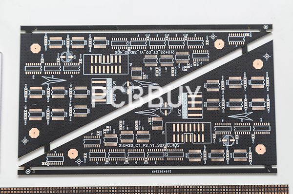
How Are Prototype PCBs Produced?
There are two main methods for prototyping a PCB:
Through-hole Technology
Through-hole technology is the traditional method of manufacturing PCBs and prototypes. This method involves inserting leads through holes on a single side of the circuit board. Then, the leads are soldered to the copper or other metal layer on the other side.
Manufacturers who use through-hole technology often make prototypes by hand. They usually have some issues because they don’t always have all of the same robust components that go into making the final version. These hand-made prototypes tend to be simple in design, and some do not last through the challenges that arise during the testing process.
Surface-mounted Technology
This method of producing a prototype is more technologically advanced. Surface-mounted technology does not need leads. Instead, the components are soldered in place usually with a speedy soldering technique.
SMT allows manufacturers to create more precise, compact boards with complex abilities. Components can be added to both sides of the board because of the soldering technique. These prototypes tend to last through testing procedures because the process makes them stronger than those made through through-hole techniques. SMT prototypes can be made quickly and efficiently.

Why to process PCB prototyping?
We recommend that you create a prototype before ordering a full production run of a new PCB design. We make sure our prototype PCB service is fast and user-friendly so you can test your board without delay or hassle. Here's what PCB prototyping enables you to do:
• Detect design flaws early in the production process before you invest significant capital
• Cost-effectively test multiple designs
• Get an accurate portrayal of how your board will function
What Are the Common PCB Manufacturing Challenges?
Electronics and PCB manufacturing is presently facing several challenges together with opportunities. Along with the need to control costs, the PCB manufacturing services will have to focus on finding ways of capitalizing on current trends. This may include integrating technologies outside their primary areas of expertise, while meeting demands from customers for highly efficient manufacturing processes that are also eco-friendly. The biggest trends and challenges in the electronics manufacturing industries are likely to be:
Manufacturing is different from designing
The design of your PCB might look good on paper or a computer screen - but it can be an entirely different story when it comes to manufacturing it.
For example, there may not be sufficient tolerances between tracks on the board, which later on in the process could result in the circuit shorting out. Or perhaps the design includes a number of components positioned closely together, each with a different thermal mass. Achieving a quality solder joint on each of these components without heat damaging the rest of the circuit board requires expert process engineering skills.
Insure the multilayer PCB stackup
Multilayer printed circuit boards are those boards that contain more than a single layer counts, hence the need for stack-up. Stack-up is the arrangement of insulating and copper layers to make a printed circuit board before the PCB layout design.

What are the main components analyzed during PCB prototype testing?
When a PCB prototype is tested, it means that the circuit design of the board is assessed to ensure it’s safe and suitable for your project. The circuit is a combination of electronic components that will be connected by conductive wires within the final PCB design and through which electrical current can flow.
These electronic components can include:
· Capacitors (C)
· Resistors (R)
· Diodes (D)
· Fuses (F)
· Inductor (I)
· Integrated Circuit (IC)
· Transistor (T)
· Relay (R)
These are the components that require testing for any faults or irregularities that could lead to PCB failure. It’s also important to ensure they are the ideal type and quality for the given project.
For example, it’s important to consider the anticipated environmental conditions (such as temperature and humidity), as well as the available current. Ask yourself: in the case of a short circuit, overload, or overheating, what’s going to happen?
Industry Category


