What Are the Common Problems of High-Speed PCB Design?
By:PCBBUY 08/29/2024 16:56
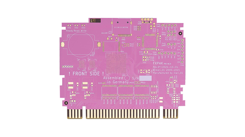
As technology advances, the demand for high-speed electronic devices continues to grow, leading to increasingly complex printed circuit board (PCB) designs. High-speed PCB design involves managing fast electrical signals that can cause various challenges. These challenges, if not properly addressed, can lead to significant performance degradation, signal integrity issues, and electromagnetic interference. This article explores the common problems encountered in high-speed PCB design and provides insights into how to mitigate these issues effectively.
1. Signal Integrity Issues
Signal integrity refers to the quality of the electrical signals as they travel through the PCB traces. Maintaining signal integrity is crucial in high-speed PCB design because even minor disruptions can cause significant data corruption. The common signal integrity issues include:
Reflections
Reflections occur when there is a mismatch in impedance along the transmission line, causing the signal to bounce back towards the source. This can lead to signal distortion and data errors.
Equation for Reflection Coefficient: The reflection coefficient can be calculated using the formula:

Mitigation: Use controlled impedance traces to ensure that the impedance is consistent throughout the trace. Proper termination techniques, such as series or parallel termination, can also be used to match the impedance.
Crosstalk
Crosstalk is the unwanted coupling of signals between adjacent traces. It occurs due to the electric and magnetic fields generated by the high-speed signals, causing interference.
Types of Crosstalk:
Near-End Crosstalk (NEXT): Interference that appears at the transmitting end.
Far-End Crosstalk (FEXT): Interference that appears at the receiving end.
Mitigation: Increase the spacing between high-speed signal traces, use ground planes to provide shielding, and employ differential signaling to minimize crosstalk.
Signal Attenuation
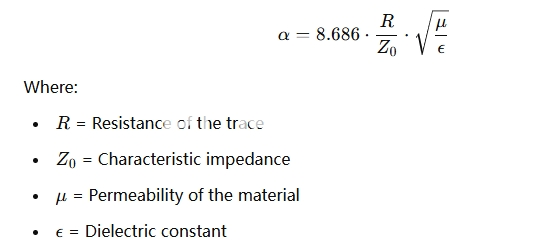
Signal attenuation is the loss of signal strength as it travels through the PCB trace. This can be caused by the resistive properties of the trace material, dielectric losses, and the frequency of the signal.
Equation for Attenuation: The attenuation in dB can be calculated using:
Mitigation: Use low-loss materials for the PCB substrate, shorten trace lengths, and optimize trace width to reduce resistive losses.
2. Electromagnetic Interference (EMI)
Electromagnetic interference occurs when the high-speed signals generate electromagnetic fields that can couple with other circuits or radiate as unwanted noise.
Radiated Emissions
High-speed traces can act as antennas, radiating electromagnetic waves that cause interference with other devices.
Mitigation: Use proper grounding techniques, such as creating a solid ground plane, and implement shielding around sensitive components. Use differential pairs for high-speed signals to cancel out radiated emissions.
Conducted Emissions
Conducted emissions refer to unwanted signals that travel through the power and ground planes, affecting other components.
Mitigation: Decouple power supply lines with capacitors to filter out noise, use ferrite beads to suppress high-frequency noise, and design a clean power distribution network (PDN) with proper grounding.
3. Timing and Skew
Timing issues arise when high-speed signals do not arrive at their destinations simultaneously, leading to data errors.
Clock Skew
Clock skew occurs when there is a delay between the arrival times of the clock signal at different components, causing synchronization issues.
Mitigation: Ensure equal trace lengths for clock signals to minimize skew. Use clock distribution techniques such as clock trees and low-skew buffers.
Data Skew
Data skew happens when data signals arrive at different times, leading to timing mismatches.
Mitigation: Use matched trace lengths for data lines, and implement timing constraints in the PCB layout to ensure synchronization.
4. Power Integrity
Power integrity refers to the stable delivery of power to all components on the PCB. In high-speed designs, maintaining power integrity is challenging due to the high current demands and switching noise.
Voltage Drops
High-speed components can cause significant voltage drops due to their high current demands, leading to power delivery issues.
Equation for Voltage Drop**: The voltage drop (V)) can be calculated using:

Mitigation: Use wider power traces to reduce resistance, employ multiple vias to lower inductance, and ensure adequate copper thickness.
Decoupling and Bypassing
Switching noise from high-speed components can cause voltage fluctuations, affecting power integrity.
Mitigation: Use decoupling capacitors close to the power pins of components to filter out high-frequency noise. Employ a combination of capacitors with different values to cover a wide frequency range.
5. Thermal Management
High-speed PCBs generate more heat due to the increased power consumption of high-speed components. Effective thermal management is essential to prevent overheating and ensure reliable operation.
Heat Dissipation
High-speed components such as processors and FPGAs generate significant heat that must be dissipated to maintain optimal performance.
Mitigation: Use thermal vias to transfer heat from hot components to heat sinks or thermal pads. Implement copper pours and planes to spread heat across the PCB.
Thermal Simulation
Thermal simulation is crucial for predicting temperature distribution and identifying potential hotspots in high-speed PCB designs.
Mitigation: Use thermal simulation tools to analyze heat distribution and optimize the placement of components, vias, and heat sinks.
6. Material Selection
The choice of PCB materials plays a critical role in the performance of high-speed designs. The dielectric properties of the substrate material affect signal integrity, loss, and thermal management.
Dielectric Constant
The dielectric constant of the substrate material affects the speed of signal propagation and impedance.
Mitigation: Choose materials with a stable and low dielectric constant to ensure consistent signal propagation.
Loss Tangent
The loss tangent indicates the amount of signal loss due to the dielectric material.
Mitigation: Use materials with a low loss tangent to minimize signal attenuation.
Thermal Conductivity
Materials with high thermal conductivity are essential for effective heat dissipation.
Mitigation: Select materials with high thermal conductivity to enhance thermal management.
7. Design Guidelines for High-Speed PCB Design
To address the common problems in high-speed PCB design, the following guidelines should be followed:
Controlled Impedance Design
- Design traces with controlled impedance to match the characteristic impedance and reduce reflections.
- Use impedance calculators and simulation tools to determine the appropriate trace width and spacing.
Minimize Trace Length
- Shorter trace lengths reduce signal attenuation and minimize timing issues.
- Place high-speed components close to each other to reduce trace length.
Use Differential Pair Routing
- Differential pairs offer better noise immunity and reduce EMI.
- Ensure that differential pairs are routed with equal lengths and consistent spacing.
Proper Grounding Techniques
- Use a solid ground plane to provide a low-impedance return path for high-speed signals.
- Minimize ground plane splits and ensure that signal return paths are continuous.
Thermal Management Strategies
- Use thermal vias and copper pours to enhance heat dissipation.
- Implement heat sinks and thermal pads for high-power components.
Power Distribution Network (PDN) Design
- Design a low-impedance PDN with proper decoupling capacitors.
- Use multiple ground and power planes to reduce noise and improve power integrity.
Conclusion
High-speed PCB design presents unique challenges, including signal integrity issues, electromagnetic interference, timing problems, power integrity concerns, and thermal management. By understanding these common problems and following best design practices, engineers can create high-performance PCBs that meet the demands of modern electronic devices. Proper material selection, impedance control, thermal management, and grounding techniques are essential for ensuring the reliability and performance of high-speed PCBs.
References
1. Hall, S. H., & Hall, G. W. (2000). *High-Speed Digital System Design: A Handbook of Interconnect Theory and Design Practices*. Wiley-IEEE Press.
2. Bogatin, E. (2009). *Signal and Power Integrity - Simplified*. Prentice Hall.
3. Johnson, H. W., & Graham, M. (2003). *High-Speed Digital Design: A Handbook of Black Magic*. Prentice Hall.
4. Montrose, M. I. (2000). *EM
Industry Category


