What Are the Considerations of Tinning on PCB?
By: PCBBUY 01/31/2024 14:57

As the name suggests, PBC tinning utilizes tin. The question is how this tin is used to mask the copper traces in a printed circuit board. The tinning process does indeed use pure tin. However, it also uses a soldered container, a mixture of lead and tin, mixed at 6:4 ratio. Pure tin and soldered tin are what make up the base of the PCB tinning solution.
Do you know how to solder tinning on PCB? In this passage, we are looking for more information about tinning on PCB, please check and read the content below in this passage.
What is the process of tinning on PCB?
As the name suggests, PBC tinning utilizes tin. The question is how this tin is used to mask the copper traces in a printed circuit board. The tinning process does indeed use pure tin. However, it also uses a soldered container, a mixture of lead and tin, mixed at a 60:40 ratio. Pure tin and soldered tin are what make up the base of the PCB tinning solution.
There are many ways to physically printed circuit board, but the most common is the electroplating method. In this method, the circuit board is placed in a tin plating station. When this happens, the tin electrodes are introduced into the controlled current flow. It completes the first coating of soldered tin.
After the printed circuit board is entirely produced, the second coating of a tin can is applied. To create the second coating of tin, even more, soldering must be done. The soldered layers of the container can be deposited either by hand or by a hot solder extruder, which will collect the soldered tin onto the area.
It will resemble liquid, which, if soldered correctly, will dry quickly as it is poured onto the copper trace. Like copper, the tin will also oxidize if exposed to outside environments. One of the reasons solder masking is applied is not to leave the circuit board unmasked.

What Are the Considerations of Tinning on PCB?
The stereotype of fluids being placed into tubes and blowing up in chemistry classes is not entirely wrong. Do not forget that printed circuit boards revolve around electric charges and generating power to and from a source. Moreover, although PCB tinning is done when a printed circuit board is not necessarily active, dangers are still involved.
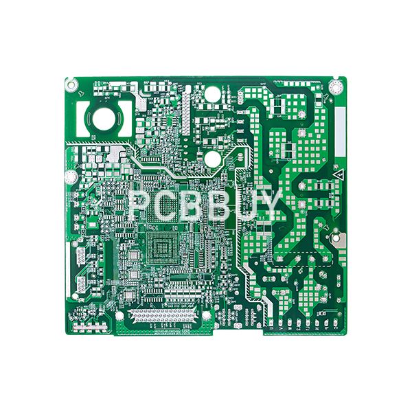
As you can see from the above picture, not only does the creation of almost anything related to a printed circuit board involve a lot of small materials, but these materials are very fragile and under much pressure.
Take tin plating chemicals such as thiourea, for example. While it will not necessarily combust when mixed, it can still contaminate food and fluids around it, and it can make these things toxic when other people who are not aware of it come in contact with it. It is made explicitly clear in this instructional guide for anybody interested in electroless tin plating.
Another precaution that needs to be taken when it comes to PCB tinning is heated. While it is unnecessary to use electrical components or heat to solder tin into a printed circuit board, heating will speed up the tinning process, as revealed in this other guide.
What are the advantages of tinning on PCB?
There are various benefits of PCB tinning that you should know about. One of the benefits of PCB tinning is the simplification of the manufacturing process as well as avoiding unnecessary etching. It is also valuable to take note that PCB tinning plays a crucial role in preventing corrosion. Normally, the process of manufacturing printed circuit boards requires the use of strong solvents such as sodium sulfate.

These solvents can be corrosive and end up damaging the components of a PCB. However, the tinning process plays a major role in ensuring the success of this process by reducing the probability of corrosion. Of great importance still, tinning helps to reduce costs associated with the manufacturing process. Generally, it is much expensive to have copper traces with a higher level of thickness on circuit boards containing smaller current spots.
How to DIY tinning on PCB at home?
It is possible for you to have a successful DIY PCB tinning. As long as you have the required tools and skills, you'll be able to get it right. However, there are precautions that you have to take to ensure that the process proceeds well. Essentially, there are a couple of things that you should take note of as you do your DIY PCB tinning. The first thing you have to always remember is that printed circuit boards have electric current flowing, so you have to be extra careful when handling them. Even when a printed circuit board is not active, it can still be dangerous to you.
Also, beware of contamination when handling tin plating materials and ingredients like thiourea. These materials can pollute foods and fluids, thus it is important for you to be extra careful when handling them. Additionally, when you're using heat in the process, you need to observe extra care. It is true that you don't have to use electrical heat to apply tin into a PCB but, if you use it, it will make the process faster. So, if you decide to use heat in the tinning process, then you have to be very careful not to cause any accidents or damage. As you know, heat is unpredictable, thus you have to be extremely careful of your surroundings.
Industry Category


