What Are the Differences Between HDI PCB and Normal PCB?
By:PCBBUY 10/31/2024 16:44

Printed Circuit Boards (PCBs) are essential components in electronic devices, serving as the backbone for electrical connections. Among the various types of PCBs, High-Density Interconnector (HDI) PCBs and normal PCBs are the most widely used. This article will explore the differences between these two types, focusing on their design, manufacturing processes, and applications.
Understanding PCB Types
What is Normal PCB?
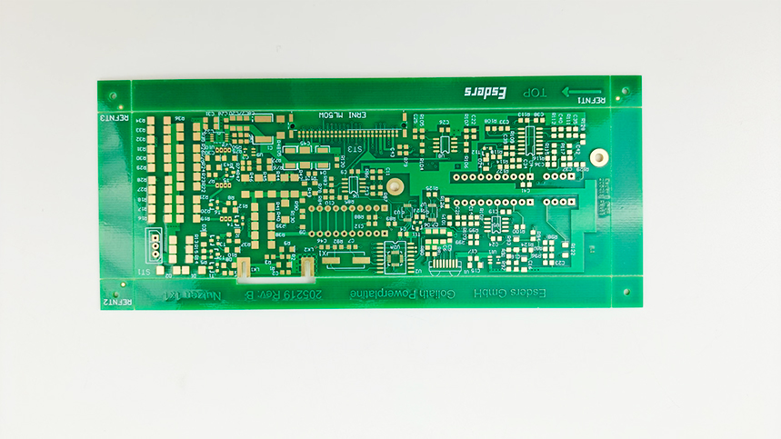
Normal PCBs, often referred to as traditional or standard PCBs, are characterized by their simple layout and structure. They typically consist of a single layer (single-sided PCB) or multiple layers (multi-layer PCB) of conductive pathways made from copper, laminated onto a non-conductive substrate. Normal PCBs are used in a wide range of applications, from basic consumer electronics to complex industrial systems.

What is HDI PCB?
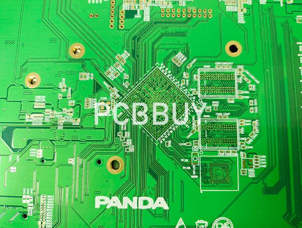
HDI PCBs, on the other hand, are designed for high-density applications, featuring a greater number of interconnections and smaller features. They utilize microvias, buried vias, and blind vias, allowing for more efficient use of space and improved performance. HDI technology supports higher circuit densities and reduces the overall size of the PCB, making it ideal for compact electronic devices.
Key Differences Between HDI PCB and Normal PCB
1. Layer Count
One of the most significant differences between HDI and normal PCBs is the layer count.
Normal PCBs can have 1 to 12 layers or more, depending on the complexity of the circuit.
HDI PCBs typically range from 4 to 20 layers, incorporating advanced manufacturing techniques to achieve high density.
2. Via Types
The types of vias used in each PCB also vary significantly.
Normal PCBs generally use through-hole vias, which pass through the entire board.
HDI PCBs utilize microvias, buried vias, and blind vias. Microvias can be as small as 0.1 mm in diameter, allowing for more connections in a smaller area.
3. Design Complexity
HDI PCBs allow for more complex designs due to their increased interconnection capabilities.
Normal PCBs are suitable for simpler designs but can become crowded as complexity increases.
HDI PCBs can accommodate more components and connections in a smaller footprint, making them ideal for high-performance applications.

4. Material Selection
The materials used in the manufacturing of these PCBs can also differ.
Normal PCBs often use FR-4 materials, which are sufficient for many applications.
HDI PCBs may utilize high-speed materials such as Rogers or ceramic substrates to reduce signal loss and enhance performance.
5. Manufacturing Processes
The manufacturing processes for HDI and normal PCBs vary significantly.
Normal PCB manufacturing involves traditional techniques such as etching and drilling.
HDI PCB manufacturing requires advanced processes such as laser drilling for microvias and fine line technology for dense routing.
6. Applications
The applications of each type of PCB differ based on their characteristics.
Normal PCBs are used in consumer electronics, industrial machinery, and general applications.
HDI PCBs are preferred in smartphones, tablets, medical devices, and aerospace technology, where performance and compactness are critical.

Performance Considerations
Electrical Performance
HDI PCBs generally offer better electrical performance due to their design.
Signal Integrity: HDI designs reduce signal paths and improve electrical performance.
Impedance Control: HDI PCBs provide better control over impedance, crucial for high-frequency applications.
Thermal Management
Thermal management is another critical consideration.
Normal PCBs may face challenges with heat dissipation, especially in densely populated designs.
HDI PCBs often incorporate thermal vias and advanced materials for improved thermal conductivity.
Conclusion
In summary, HDI PCBs and normal PCBs serve different needs within the electronics industry. HDI technology enables more complex designs, better electrical performance, and smaller form factors, making it ideal for modern high-density applications. Understanding these differences is crucial for engineers and designers when selecting the appropriate PCB for their projects.
References
- [Reference 1: PCB Design Fundamentals]
- [Reference 2: HDI PCB Technology and Applications]
- [Reference 3: Advanced PCB Manufacturing Techniques]
Industry Category


