What Are the Difficulties in Heavy copper PCB ?
By:PCBBUY 12/24/2024 14:42

With the rapid development of China's automotive electronics and power communication modules, heavy copper printed circuit board has gradually become a special printed circuit board with broad market prospects, in automotive electronics, IGBT (insulated gate bipolar transistor) installation, wind power converter, ignition coil and other aspects are in demand: in addition, with the wide application of printed circuit board in the field of electronics.
The printed circuit board will not only provide the necessary electrical connection and mechanical support for electronic components, but also gradually be given more additional functions, so can integrate the power supply, provide high current, high reliability of the ultra-heavy copper multi-layer printed circuit board has gradually become a new product developed by the printed circuit board industry, with broad prospects. The profit margin is larger than the traditional circuit board, and it has a very large development value. Ultra-heavy copper multilayer printed circuit boards will occupy an important position in the future high-end circuit connection market, and will inevitably usher in a broader market prospect.
What Are the Difficulties in Heavy copper PCB Manufacturing?
Under normal circumstances, printed circuit boards with a thickness of 105um and above (including electrolytic copper pins after surface treatment and calendered copper foil) are collectively referred to as heavy copper boxes. According to the thickness of the pin, it can be divided into three types: 10Sm~300m is called heavy copper foil 300 ~600um is called super heavy copper foil 600m and above is called super MAX copper pin. Printed circuit boards made of heavy and ultra-heavy copper foils can be called "heavy copper printed circuit boards". It uses conductive materials (copper foil) and substrate materials, production processes, application areas are different from conventional printed circuit boards, so it is a special printed circuit board.
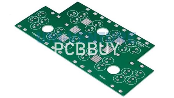
The application field and demand of heavy copper printed circuit board have been rapidly expanded in recent years, and it has now become a kind of "hot" printed circuit board product varieties with good market development prospects. In the manufacturing process of heavy copper printed circuit board, there are more manufacturing process differences with ordinary printed circuit board manufacturing. It is mainly reflected in the etching of heavy copper foil, the lamination of heavy copper foil, the drilling of heavy copper foil and the printing resistance soldering of heavy copper foil.
1. Etching problem of heavy copper foil
The etching of ultra-heavy copper will cause a large side corrosion problem, so that the etched line profile presents a "long trapezoid" or even a triangular structure, resulting in a great difference from the design of the printed circuit board. Therefore, reducing excessive engraving of ultra-heavy copper foil is a difficult problem faced by heavy copper printed circuit boards.
2. Lamination problem of heavy copper foil
Due to the heavyer copper foil of the inner core plate, compared with ordinary heavy copper foil, the amount of resin that needs to be filled with heavy copper foil is greatly increased, which poses a great challenge to the resin load material and the corresponding processing technology to achieve the true filling function:
1) The resin content that can be carried by traditional semi-cured sheets is limited. Although the superposition method of multiple thin semi-cured sheets can meet the overall resin content demand, there is still a high probability of pressing holes caused by insufficient filling
2) Some filling positions will have small cracks due to incorrect filling, and cracking will occur after thermal stress
3) In the vertical flow process of the resin penetrating through the glass fiber cloth to the lower layer to be filled with glue, due to the filtration effect of the glass cloth, the uniform distribution of the resin and the filler is destroyed, and the local filler is more and less resin, and the heat resistance of the corresponding filling position may be deteriorated.
4) During the pressing process, the glass fiber cloth displaces and forms a stress concentration point close to the sharp Angle of heavy copper. Due to the inconsistency between the thermal expansion coefficient of copper foil, resin and glass fiber cloth during thermal shock, the stress concentration point produces a "crack" problem
3. Drilling problem of heavy copper foil
Because the copper foil is heavy and the heat is large, it often brings cracks and other defects to the quality of the hole wall, and also puts forward greater difficulty and challenge to the drilling process
4. Seal resistance soldering problem of heavy copper foil
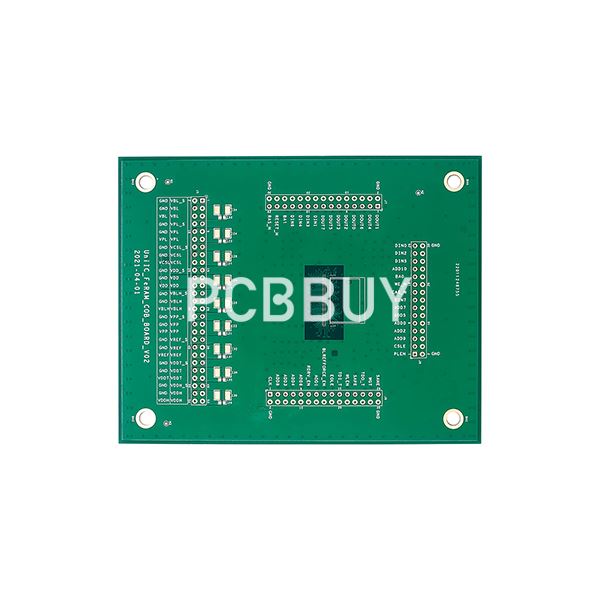
If the positive soldering wire printing is carried out according to the ordinary multilayer printed circuit board, it is difficult to cover the line well due to the insufficient amount of positive flux in the screen printing. If the dose of solder resistance ink is increased, the ink is easy to produce bubbles when filling heavy lines, resulting in difficulties in meeting the requirements of T art
What Are the Key points of manufacturing process of heavy copper PCB?
At present, the manufacturing process of heavy copper printed circuit boards is basically the same as that of ordinary multi-layer printed circuit boards, but there are differences with ordinary printed circuit boards in some key processes. In terms of solving key processes, each manufacturer has its own processing methods. The following from the heavy copper printed circuit board manufacturing problems of the product process points are introduced.

1. Heavy copper etching technology
Heavy copper etching takes a longer time to complete the etching process. Therefore, in the etching process, the lateral erosion also becomes very serious. To solve the problem of lateral erosion is to solve the problem of lateral erosion. At present, the methods to solve the side corrosion are side etching inhibition method and double side etching method.
(1) Side etching inhibition method
Adding wetting agents and corrosion inhibitors to the etching solution can reduce the side corrosion of the etching solution to the line. Etching fluid wetting agent is a kind of organic matter that reduces the interfacial tension between etching fluid and copper surface, which can make the etching fluid fully contact with the copper surface and improve the etching rate. Corrosion inhibitor is a kind of organic matter that can be adsorbed on the surface of copper.
The mode of action of this additive is that the adsorption amount of corrosion inhibitor in different parts of the copper surface is different due to the tip adsorption and the difference in spray pressure on the front and side of the line, which leads to the amount of corrosion inhibitor adsorbed on the side of the line being larger than that on the front, resulting in a lower etching rate on the side than that on the front, resulting in a smaller corrosion quantity on the side, which is presented as an increase in the etching factor. For example, adding the corrosion inhibitor benzotriamine breakdown to the etching solution increases the etching factor to 3.0. If the corrosion inhibitor and wetting agent can be well designed, the etching fluid can maintain the side corrosion within 2wm, and the etching factor is improved from the root. Therefore, the future direction of exploration of heavy copper acid etching fluid for printed circuits is to constantly pursue new acidic etching fluid additives.

(2) Double-sided double etching
Heavy copper lines are not only difficult to etch once, but also very difficult to form and press. In order to solve the above problems, the heavy copper foil material is directly used for step-by-step controlled etching technology, that is, the copper foil is first etched on the reverse side of 1/2 thickness, and then pressed together to form a heavy copper core plate, and finally the front etching to obtain the inner circuit pattern. Because of the step etching, the difficulty of etching is greatly reduced, and the difficulty of pressing is also reduced. For double-sided secondary etching method, two sets of photographic substrates are designed for each layer of line file. The image of the first etching should be mirrored to ensure that the line is in the same position when the forward/reverse control deep etching, and no dislocation will occur.
Primary etching
In order to ensure the overlap of the two lines, the expansion and contraction value should be measured after the first lamination, and the expansion and contraction compensation of the line should be adjusted. It is best to use laser direct imaging automatic alignment, which effectively improves the alignment accuracy. After optimization, the alignment accuracy can be controlled within 25um. In order to improve the etching quality of ultra-heavy copper lines, alkaline etching and acid etching are respectively used for comparative testing.
2. Heavy copper lamination technology
Heavy copper lamination first needs to solve the problem of glue flow, that is, the implementation of glue resistance technology. The object of blocking flow in the blocking adhesive is the semi-cured sheet resin. When the temperature is 80 ~140C, the resin is converted from the semi-cured state at room temperature to the liquid state, at this time under the action of laminating machine h, the resin in the liquid state spreads to the four sides. Therefore, the structure of the process edge design of the inner layer heavy copper plate includes the wall brick process edge, the PAD mode process edge and the mixed process edge. In order to fill the glue between the lines, the multi-layer heavy copper plate needs to ensure that the plate thickness is within the required range, and the resin content and the semi-cured sheet of fine glass fiber cloth are selected as far as possible.
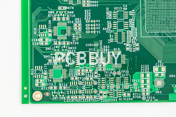
In terms of uniformity control, it is necessary to use silicone as the key buffer layer in the spring pressing process, which plays the role of uniform distribution of pressure in the pressing. If the lamination problem can not be solved by changing the lamination parameters, it is necessary to fill the resin between the high-thickness copper lines with pre-coated resin or powder particles, and then semi-cured laminate, prefilled with liquid solid resin powder to meet the high filling requirements, and then supplement with semi-cured sheets with high resin content to meet the requirements of fine filling. It can also reduce the problem of crack caused by stress after lamination of glass fiber cloth reinforced semi-cured sheet.
3. Heavy copper drilling technology
In order to solve the heat dissipation problem of heavy copper, the feed speed, drilling rate and withdrawal speed of the drilling hole should be properly illuminated. The range of reduction is adjusted according to the thickness of the steel pin. When stacking, it is also necessary to reduce the thickness of the stacking, and it is recommended that only two boards be stacked at a time of drilling.
You can also adjust the cover plate to solve the problem of heat dissipation. The water-soluble substances on the cover surface of the cover can infiltrate the drill tool when the tool is advanced and withdrawn. The drill knife can be cooled at high temperatures, and the water-soluble substance evaporates into a gas.
In addition, when drilling, pay attention to prevent the copper in the hole, drilling parameters should be properly reduced according to the machine and other conditions, to prevent broken bits and machine displacement.
4. Heavy copper solder resistance technology
Soldering resistance production is a difficult point, because the copper thickness is too heavy, the base material and copper have a large drop, the screen printing can not be reached, the scraper push 1 to 2 times to fill the soldering resistance oil with the base material, but pushing the scraper too many times will cause the ink to enter the hole, so we must first make a file point screen only print the base material position. Check the screen printing effect after printing 2 to 3 times in different directions. If the substrate is not filled, print white paper to clean the screen plate. Then print two knives in different directions to check.

After each plate is printed, it is necessary to print the white paper to clean the screen plate and then print the next one, so as to avoid ink manholes. After printing, it must be placed horizontally for more than 4h to pre-roast before the last printing resist soldering. The soldering resistance ink of the early printing is mainly used to smooth the surface of the plate to facilitate the dry film to be tight in the later period, so the height of the ink and the height of the copper surface should be consistent as far as possible.
Recommended resist soldering production process: using only substrate screen printing single side substrate one side white screen printing one side exposure one side development one test one side curing one side substrate using only substrate screen printing one side white screen printing one side static one prebake one side exposure one development one test one cure one second double print resist soldering one normal production
Reference
He Wei, PCB Basic Electrical Information Science and Technology, China Machine Press,341-344
Industry Category


