What Are the Essential Tips to Check PCB Quality Using 10 Effective Methods?
By:PCBBUY 07/04/2023 15:44

The Design Rules Check (DRC) is a very important step in PCB quality control. When we receive a new PCB order from a customer, we will use an automated tool to verify that the layout does not have any specific placement, routing or other addressable layout errors.?
How to check the quality of PCB during the whole manufacturing process? If you are curious about it, please check and read the content below for more information.
Confirm the quality of PCB
PCB designers have to check and confirm the design drawings that will be applied by manufacturer for many times prior to manufacturing. Since PCB design can't be successful just after one trial and modifications have to be made time and time again, PCB manufacturers will hold multiple versions of design drawings. So it's necessary to carefully check and confirm the final design drawing provided by manufacturer prior to practical manufacturing so that manufactured PCBs conform to requirement of the last version.
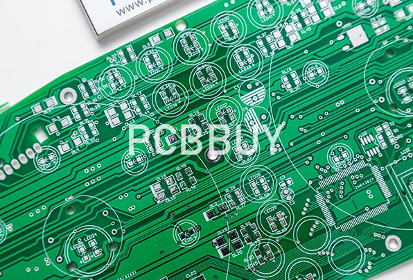
Inspect Traces in your PCB Design
Traces are wire conductors responsible for current flow from one component to another. In your PCB- the solder masks cover up the particles. A good practice to reduce errors is color-coding the masks. Traces of only the top and bottom layers of your PCB designs are visible. The usual solder mask color is green- although other colors are also available. White is difficult to notice.
Errors due to Trace misplacement are common. The usual golden rule is- Keep the trace connections as clean as possible. Traces with sharp bends can be problematic for higher power or frequency transmission. Try to avoid steep 90-degree angles. There are exceptions to this general rule too. PCBs with square concentric spirals are a perfect example. We can find these characteristics of high-quality PCB.
AOI to check the PCB quality
Typical AOI inspection technologies currently used in circuit board manufacturing include: film inspection, drill inspection, hole location inspection, circuit inspection, blind hole inspection, bump inspection, visual inspection, etc.

At present, the most used AOI inspection technology in the circuit board manufacturing industry is the inspection of the appearance of the circuit board. Although the size of the circuit characteristics of the circuit board has been reduced by more than ten times, the optical system and the matching hardware and software systems have also made great progress.
CAF resistance in PCB
Conductive Anodic Filament (CAF) has been increasingly concerns on printed circuit boards in the last few years. The major factors are current trend toward smaller size, lighter weights, thinner and higher performances that the density of PCB shall be designed with more closely spacing conductors, much smaller pitches and single-ply dielectrics such as mobile telephones, notebook computer and camcorder. In the other hand, some electrical applications must be exposed in extreme environment. For example, the safe necessity of automotive like engine control and brake control system. There cannot occur electrical shorts phenomenon, so the insulation resistance of material becomes very importance. These factors are pushing the demand for anti-CAF materials.
Requirements of PCB assembly
PCBA quality will depend on your CM’s manufacturing process, especially its adherence to industry standards. And while PCBA performance and reliable operation are primarily design issues, structural integrity and component mounting—as well as the mechanical ability of your boards to remain intact over their projected operational lifecycle—are CM responsibilities that define board quality and contribute significantly to operational reliability.
Be sure to include the board revision and other identifiers, such as publishing date, that clearly distinguish this design. Specify any components or areas of your board that need special attention—for example, polarization, moisture sensitivity and keep-outs. Ensure that any process or readability requirements for silkscreen layer reference indicators, labels and markings are included.
Flying Probe Testing
The flying probe test method is the latest solution in electrical testing. It uses a generic board holder along with one or more probes. Under software control, these probes access all the nodes on the board one by one. This allows testing for opens, near opens and shorts.

Flying probe testers can now perform onboard memory module programming along with checking for opens and shorts, and test components like diodes and transistors junction. Some advantages of the flying probe test are that requires no test fixture and little set-up time.
The drawbacks to this test are:
· lower test speeds compared to in-circuit
· incompatibility with the complex circuits
Bed of Nails / Universal Grid Testing
The universal grid is also known as clamshell or bed of nails fixture test. Just as the name describes, the electronic fixture for universal grid testing has numerous pins inserted into holes in an epoxy phenolic glass cloth laminated sheet.
These holes are then aligned to the test points on the printed circuit board using tooling pins. This type of testing is used when there is a large production of PCBs. In the universal grid process, all the test points are checked at the same time.
Industry Category


