What Are the FPGA PCB Design Guidelines during Manufacturing?
By:PCBBUY 04/29/2022 14:00

Assuming this design will be either a prototype run or possibly a small production run, it makes sense to design your PCB with specific requirements in mind to keep costs reasonable. The two PCB specifications you are most commonly told are the minimum “trace/space” (that is, minimum width of a trace, and minimum spacing between copper features), and the minimum drill size.
Are you going to learn more knowledge of FPGA PCB design? If you are curious about the FPGA PCB design and need the guideline, please check and read the content below in this passage.
What are working principles of FPGA PCB design?
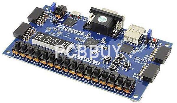
FPGAs have an “array” of integrated hardware circuits — these arrays are groups of programmable logic blocks. During manufacturing, an FPGA has not been configured to have any particular function. Instead, the user can configure it and later reconfigure it however they choose.
The user does this using a hardware description language (HDL). An FPGA has logic blocks, like AND and XOR, which the user can piece together with interconnects. Modern FPGAs have many logic gates and RAM blocks, so they can accommodate complex computations. Some FPGAs also have analog-to-digital converters or digital-to-analog converters, similar to field-programmable analog arrays (FPAAs).
How to design FPGA PCB?
The chronological progression of an electronic design is an interesting one and also not a uniform one. The process in many industries on how to make something or how to do something is usually fairly well defined.
If you take building a road for example, then the usual process is to; plan the road, design the road, conduct the earthworks needed to build the road, and then pave the road. This process is fairly linear, in that you can’t pave the road before doing the earthworks and you can’t do the earthworks before doing the planning (unless you don’t mind getting it wrong!).

In electronics design now this is not the case, and especially with FPGA designs.
Just as an example, the development of the FPGA’s constraints may have to begin before the component is connected in the schematic. This may be because the pin function is limited to certain pins. Maybe the FPGA IO has to be configured in a certain way for the part to work which is required by the firmware. Either way, this is a problem which requires swapping back and forth between developing the schematic of a board/product and developing the firmware for it.
There is an interesting nuance to this situation however. This means that you can’t finish the schematic before doing some firmware, but you can start the schematic before the firmware. Based on that, this is where we start too.
The Schematic
The schematic capture of a design usually comes when all of the required information about what the PCB is meant to do is available. This is key to the success of a design because, otherwise, you don’t know what you’re designing.
Just a quick note for those of you who are completely unaware of the PCB design process, a schematic is a drawing used to define the interconnect between the components that make up the design. In order to draw the schematic that we need, we also need some software to do it. We use KiCad in house at Circuithinking which is an excellent free software package used at CERN. We highly recommend that you go and have a look or even have a try at the tools they provide.
Some loose requirements were established in the first article and now we can begin to design a board to meet those requirements. If you choose to use Circuithinking as your design service, then we can use our extensive systems in order to provide you with great quality requirements and documentation so that you can maintain your product for years to come. The first step is to architect our design so we know what components we are using.
What are the applications of FPGA PCB?
The Altera series FPGA boards are a multiuser, multi-threaded design suited for many markets such as enterprise automation, digital signal processing, and cyber security. These series include FPGA devices with a comprehensive range of I/O expansion for processor-intensive applications. They include:

Intel Stratix 10 FPGA board:
If you need a compact, powerful FPGA for various engineering applications in various industry sectors, this is your board. FPGA boards are helpful in many different applications, including embedded system design and video processing.
Intel Stratix Ge FPGA board:
This board is specifically designed for the aerospace industry, whereas the Stratix 10 FPGA board is a more general-purpose FPGA. The Ge FPGA board has a bit more computational performance and throughput than the Stratix 10 FPGA board. This board can handle a wide range of applications. The board is also suitable for professional design projects.
Industry Category


