What Are the Features of High Voltage PCB?
By:PCBBUY 09/30/2024 16:32
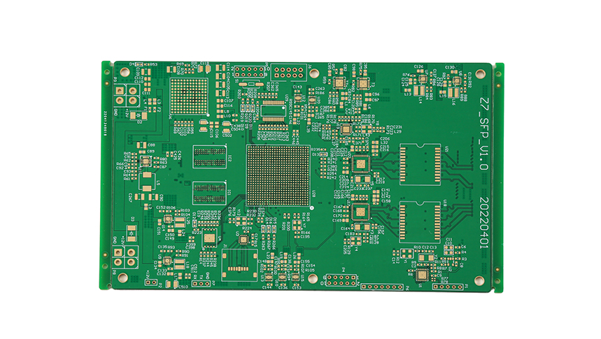
High voltage PCBs (Printed Circuit Boards) are specialized boards designed to handle high electrical voltages safely and efficiently. These boards are crucial in various applications, including power supplies, electric vehicles, renewable energy systems, and industrial equipment. This article explores the unique features of high voltage PCBs, the materials used, their design considerations, and the manufacturing processes involved.
1. Understanding High Voltage PCBs
1.1 Definition of High Voltage PCB
A high voltage PCB is specifically engineered to withstand voltages typically greater than 1,000 volts. These boards must prevent electrical arcing and ensure that components function correctly under high stress.
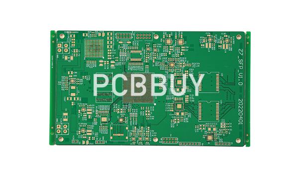
1.2 Applications of High Voltage PCBs
High voltage PCBs are used in:
- Power conversion and distribution systems
- Electric vehicles (EVs)
- Renewable energy systems (solar inverters, wind turbines)
- Industrial machinery and automation
2. Key Features of High Voltage PCBs
2.1 Material Selection
The choice of materials is critical in high voltage PCB design. Key materials include:
Dielectric Materials: High dielectric strength materials like polyimide or FR-4 are commonly used to prevent breakdown.
Copper Thickness: Thicker copper layers are often utilized to handle higher current loads and reduce resistive heating.
Table 1: Comparison of Dielectric Materials
|
Material |
Dielectric Strength (kV/mm) |
Advantages |
Disadvantages |
|
FR-4 |
20-30 |
Cost-effective |
Limited temperature range |
|
Polyimide |
20-50 |
High thermal stability |
Higher cost |
|
PTFE |
50-60 |
Excellent chemical resistance |
Expensive |
2.2 Design Considerations
2.2.1 Spacing Requirements
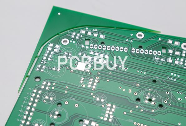
High voltage PCBs must adhere to strict spacing requirements to prevent arcing between conductive paths. The spacing is determined by:
Voltage Levels: Higher voltages require increased spacing.
Environmental Conditions: Factors like humidity can influence spacing requirements.
2.2.2 Component Placement
Careful placement of components is essential to minimize the risk of electrical failures. Key considerations include:
Thermal Management: Components generating heat should be spaced adequately to allow for heat dissipation.
Electrical Isolation: High voltage components must be isolated from low voltage areas.
2.3 Surface Finish
The choice of surface finish can impact performance and reliability. Common finishes include:
HASL (Hot Air Solder Leveling): Good for standard applications but may not be suitable for high voltage due to surface irregularities.
ENIG (Electroless Nickel Immersion Gold): Provides a flat surface and better reliability for high voltage applications.
3. Manufacturing Processes
3.1 PCB Fabrication
The fabrication of high voltage PCBs involves several key steps:
1. Design and Layout: Using specialized CAD software to create layouts that adhere to high voltage standards.
2. Material Preparation: Selecting and preparing appropriate dielectric and conductive materials.
3. Layer Stacking: Configuring layers to achieve the desired electrical and mechanical properties.
3.2 Testing and Quality Control
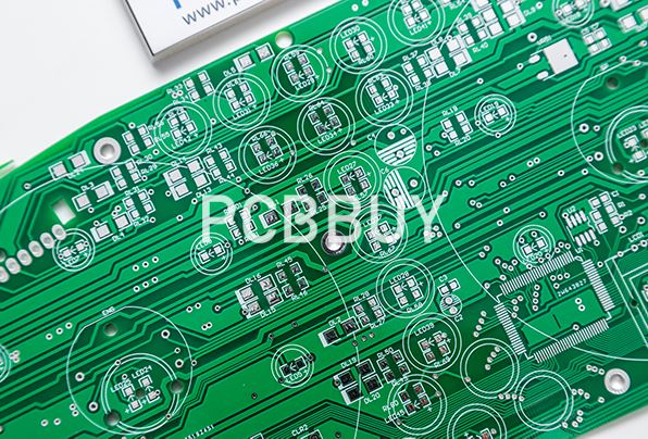
Testing is critical to ensure high voltage PCBs function as intended. Common tests include:
Dielectric Testing: Verifying that the insulation can withstand the specified voltage.
Thermal Cycling: Testing the PCB under temperature variations to assess reliability.
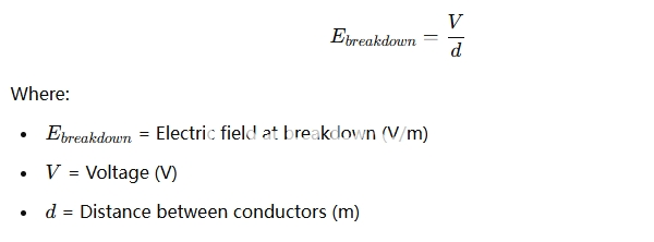
Chemical Equation for Dielectric Breakdown
The dielectric breakdown can be modeled using the following relationship:
4. Safety Standards and Regulations
4.1 Industry Standards
High voltage PCBs must comply with various industry standards, including:
IEC 60950: Safety of information technology equipment.
UL 60950: Standard for safety of information technology equipment.
4.2 Compliance Testing
Manufacturers must perform compliance testing to ensure that high voltage PCBs meet safety regulations. This testing often includes:
High Voltage Testing: Assessing the PCB's ability to withstand high voltages.
Environmental Testing: Evaluating the PCB's performance under various environmental conditions.
5. Future Trends in High Voltage PCB Technology
5.1 Advancements in Materials
The development of new materials, such as nanocomposites and advanced ceramics, is expected to enhance the performance of high voltage PCBs. These materials may offer improved thermal management and dielectric properties.
5.2 Integration with Smart Technologies
The integration of smart technologies, such as sensors and IoT capabilities, into high voltage PCBs is on the rise. This trend aims to improve monitoring and control of electrical systems.
Conclusion
High voltage PCBs are essential components in modern electronic systems, particularly in power management and energy conversion applications. Understanding their unique features, including material selection, design considerations, and manufacturing processes, is critical for engineers and manufacturers. As technology advances, high voltage PCBs will continue to evolve, offering improved performance and reliability for various applications.
References
1. IPC. (2021). "Design Guidelines for High Voltage PCBs." IPC.
2. IEEE. (2022). "Standards for High Voltage Equipment." IEEE Standards.
3. Rogers Corporation. (2023). "Materials for High Voltage Applications." Rogers Corporation.
4. Friedman, A. (2024). "Future Trends in PCB Technology." Journal of Electronics.
5. Hwang, J. (2022). "Safety Standards in High Voltage PCB Manufacturing." International Journal of Electronics.
Industry Category


