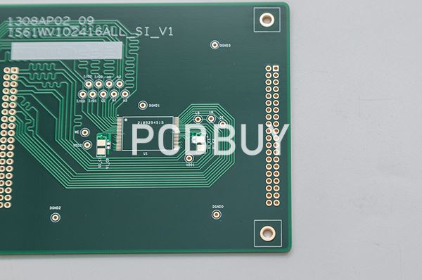
What Are the Features of Protel PCB?
By:PCBBUY 02/29/2024 15:57

Protel PCB has been available since the 1980s. It is an important tool for PCB designers. It tests, verifies, and completes PCB design concepts. This software is one of the best EDA software. This software is very old and as such, requires a virtualization tool to run.
In this passage, we will provide all the information about Protel PCB design. If you are going to learn more about the knowledge of Protel PCB design, please check and read the content below in this passage.
Why to use Protel PCB?
Protel software pcb is a comprehensive and modern solution specifically created for PCB designers. This software is the best choice among designers and engineers across the world. It is well known for its accuracy and efficiency in designing PCBs. This software represents years of development and innovation.
This cost-effective and easy-to-use software helps to make PCB designs accurately. Protel launched PCB 1.0 in 1991 and between 1991 and 1993, it launched PCB 2.x. Protel98 was launched in 1998. Protel has launched several versions ever since. It is now rebranded as Altium Designer.
What Are the Features of Protel PCB?
Protel is one of the first PCB software designed for personal computers. This software has continued to pioneer innovative tools that are useful in all aspects of the design process of a PCB. Protel, which is now known as Altium designer, has gained more than 30 years of experience in making great designs for PCB. This software offers some features which include;
Advanced route and place tools
Protel features great reroute and place tools. This is one of the integral features of its design system. These tools are now more advanced in Altium designer. You can easily position and organize your components with smart placement algorithms.
Improved utilities and functionality
Protel PCB helps you stay competitive. This software helps designers to route circuit board track much faster. It features Active BOM that helps you to directly evaluate component data and select the components into the PCB layout.
Unified Interface
Protel software PCB is specifically designed to deliver powerful designs to engineers and designers. This software is an effective application that contains advanced design tools needed to help you achieve a great design. The interface is very easy to use for both experts and newbies.

How to process of Protel PCB design?
Building a digital twin, virtual model of the 2.5D/3D heterogeneous assembly provides a comprehensive representation of the full system comprising multiple devices and substrates. The digital twin enables automated verification of heterogeneous assemblies beginning with substrate-level design rule checking (DRC) and expanding into layout versus schematic (LVS), layout versus layout (LVL), parasitic extraction, stress and thermal analysis, and, finally, test.
One of the primary benefits of the digital twin approach is that it serves as the golden reference to drive complete physical and electrical verification at every level of the design hierarchy. That eliminates using multiple, static spreadsheets to represent pin and connectivity information, replacing them with a full, system-level netlist in Verilog format.
The preservation and reuse of original data, such as a device’s Verilog description, is key. The biggest risk comes when translation or conversion occurs, such as with a schematic or spreadsheet. If this is done, the “digital thread” is immediately broken, and the risk for connectivity errors skyrockets.

What are the advantages of Protel PCB?
Protel PCB is software specifically designed for engineers. This software has a lot of benefits discussed below;
User-friendly
Protel PCB is ideal for both experts and novices since it is very easy to understand and use. This software’s tools come easy. The exporters, importers, and other tools can be used by any designer. Unlike other PCB software, the Protel design system is user-friendly. This software features easy-to-use tools, design templates, and a well-detailed library of components.
Reduces design complexity
This software simplifies design complexity. It makes use of a schematic and this schematic starts with selecting the right parts. You can identify and import vendor components in your design from the cloud. Engineers can design circuits on multi-layer and single-layer boards. Protel PCB simplifies complex designs into logical ones.
Saves costs on production
Protel PCB helps designers to save costs of production that could have been spent on designing physical prototypes. Quick virtual prototyping via the utilization of software tools enables manufacturers to commit resources and labor to a cost-efficient model for the final product.

How to avoid the common mistakes of Protel PCB design?
PCB designers must be able to develop excellent layout designs for the proper functionality of components that use printed circuit boards. Lately, there is a huge demand for PCBs with minimal footprints. Printed circuit board designers are therefore required to employ the use of smaller components that reduce footprint significantly. Generally, components that find use here are very close to each other.
Clogged roadways are similar to a PCB that does not account for the high amount of charge trying to pass through a far too narrow trace. A too-narrow trace for a particular current is likely to act as gridlock by starving components reliant on that power net of the current flow necessary for operation. Such a problem becomes far more sinister than runtime errors. Excessive heat can lead to board warpage, delamination, and other board failure modes that are likely to lead to scrapping. High current PCB practices need to be employed to keep a board in operation but functioning in lockstep with its design intent to avoid any issues during prototyping or field use.
Industry Category


