What Are the Features of Tooling Hole in PCB?
By:PCBBUY 11/03/2023 16:35

If you’ve ever visited a PCB production facility, you’ll find that it’s filled with machines for the entire manufacturing flow. These machines turn a PCB manufacturing file into a physical PCB, and later, populate it with components. Precision is key to ensure that the final product is free from issues—PCB tooling holes design plays an important role in this.
Besides size, you’ll also need to ensure that the PCB tooling hole isn’t plated. A non-plated hole is better in terms of accuracy compared to a plated one. Also, ensure that there is a solder mask expansion that slightly extends over the hole. In this passage, please check and read the content below for more professional information about tooling Hole in PCB.
What Are the Features of Tooling Hole in PCB?
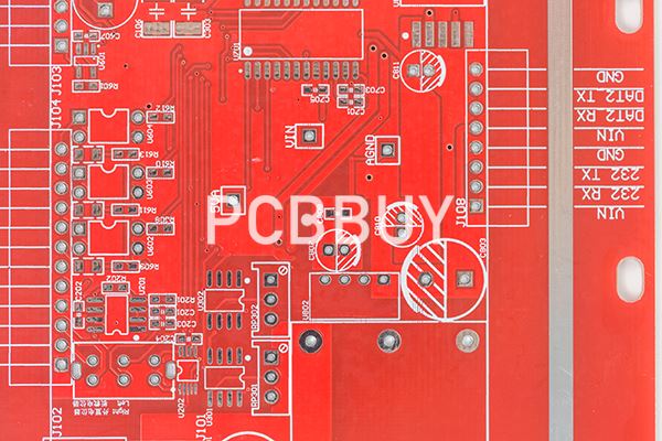
PCB tooling holes, or mounting holes, are circular openings made at the edge of a PCB. Tooling holes are non-plated, and they are used by machines to hold the PCB down for alignment. During the fabrication process, it’s imperative that the PCB be kept still and properly aligned for drilling. If the PCB is not kept still, it will be impossible to deliver precisely-drilled holes.
When the fabricated PCB is sent for assembly, the tooling holes will be needed again if there are SMD components in the design. The machines will use the tooling holes for stencil alignment when applying solder paste and placing SMD components with the pick-and-place machines.
It is important to note that PCB tooling holes should not be confused with fiducial markers. Fiducial markers are pads that are created on the PCB to provide a reference for optical pick-and-place machines. However, both are equally important when designing a PCB with SMD components.

How to work with tooling Hole in PCB?
Tooling holes will probably be one of the simplest features in your PCB, but they are critical for fabrication and assembly. There are three main points to consider when determining where and how to place tooling holes in your PCB:
· Placement during panelization
· Size and plating
· Placement with fiducials
How to process tooling hole in PCB?
Usually, common sizes like 1mm, 1.5mm, and 2mm are acceptable tooling hole sizes for most manufacturers. If you’re unsure, make sure to consult with your PCB manufacturer. For uniformity, you’ll want to stick with a common size for all tooling holes on a PCB.
Besides size, you’ll also need to ensure that the PCB tooling hole isn’t plated. A non-plated hole is better in terms of accuracy compared to a plated one. Also, ensure that there is a solder mask expansion that slightly extends over the hole.
PCB fabricators use them for aligning the board during drilling and routing. Assemblers use them
For alignment with stencils during solder paste printing, and for location on pick-and-place machines. They are used for alignment on electrical test fixtures. They may also be used as alignment holes in the final enclosure, often mating with small moulded plastic posts.

What is the creation of tooling Hole in PCB design?
If tooling holes are needed in the board for any manufacturing processes, the PCB contract manufacturer may request they be added to the design. Typically the CM will either use holes that are already on the board or add their own to the fabrication files. Creating the holes used for mounting hardware is a different matter, and they must be made with the correct design parameters to function as expected:
· Location: The number of holes used for tooling and where they are located is dependent on what the circuit board and its components require. Component datasheets typically specify the location of these holes for the designer to include in their PCB footprints.
· Preferred size: This again is dependent on the requirements of the components. Usually, these parts will use 4-40 or 6-32 screws, and the holes must be drilled to match the mounting hardware. If no system mounting holes have been included in the design, PCB CMs will recommend adding some holes with a generic size of 0.100 or 0.125 inches to give their clients mounting options for the future.
· Plating: This is also dependent on the hardware’s needs that will be attached to the hole. For hardware that needs to be connected electrically to the board, the hole must be plated and connected to the appropriate net. Otherwise, a non-plated hole will be used.
· Plane connections: A plated hole connected to either a power or ground plane must not be connected to any other planes to prevent shorting power and ground nets together. While CAD tools have net checking built into them to prevent this, incorrectly designed mounting holes may end up fooling design rule checks.
Industry Category


