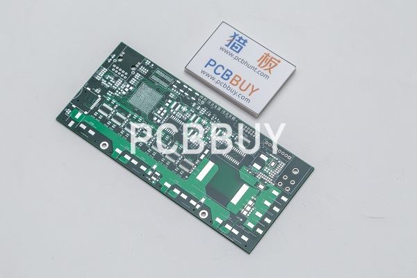
What Are the Functions of A PCB Stencil in PCBA Process?
By:PCBBUY 05/05/2023 14:32

Before you can go into production, solder paste is printed onto the component pads of the PCB. How can you make sure you apply the solder paste with precision exactly where it needs to go? Stencils, or formally surface mount technology stencils, are the answer. Stencils are the medium used to transfer that solder paste onto the PCB.
What is the basic definition of PCB stencil?
The sole purpose of an SMT stencil is to transfer solder paste to a bare circuit board. A stainless steel foil is laser cut creating an opening for every surface mount device on the board. Once the stencil is properly aligned on top of the board, solder paste is applied over the openings (making a single pass, using a metal squeegee blade). When the stainless steel foil is separated from the board, solder paste will remain, ready for placement of the SMD. This process, as opposed to hand soldering methods, ensures consistency and saves time.
What is the standard thickness of PCB stencil?
This is important to ensure there is good release of solder paste from the apertures and to obtain the correct volume of solder paste to achieve the desired solder joint. Typically the stencil thickness would be between 4 thou and 8 thou thick. If the stencil is too thick for the size of apertures then it can lead to the paste being held by surface tension to the inner walls of the aperture.
What are the types of PCB stencil?
The PCB stencil is utilized to store bind glue on assigned spots on an uncovered PCB board so that parts can be appropriately set and be entirely adjusted on the board. The fundamental feature and purpose of a PCB stencil are to precisely store the perfect measure of solder paste on SMT cushions for the weld joint between the cushion and the part to be appropriately structured concerning the electrical connection and mechanical strength. Utilizing a PCB Stencil to put solder paste makes the PCB Assembly process quicker and more efficient.
· Hybrid PCB Stencils
· Prototype or Photo PCB Stencils
· Frameless/ Reusable PCB Stencils
· Framed / Framework PCB Stencils
· Chemical-etch PCB Stencils
· Laser-cut PCB Stencils
How to process PCB stencil?
PCB Stencils are produced by making openings or apertures through laser beams on a hardened steel foil-based sheet at the positions where Surface Mount segments are to be set on the circuit board. The Stencil is then positioned on the head of the PCB circuit board and adjusted properly utilizing certain focuses called fiducial imprints.
After arrangement, the solder paste is applied with a metal tool cutting edge. According to the size and position, the solder paste gets set on the PCB circuit board where the surface mount parts should be placed according to their position. So, when the PCB stencil is evacuated, parts can be set on the board in their determined position properly.

What are the factors of PCB stencil design?
The following is a breakdown of the critical elements of stencil design:
Stencil Thickness
It is another crucial determinant of a stencil’s capacity to release the solder paste. If the thickness isn’t suitable for the size of apertures, you’ll not achieve the required solder joint. In this case, the paste may adhere to the inner walls of the cracks due to surface tension.
Aperture Design
The aperture design can affect the solder joints in many ways. First, it determines the chances of the occurrence of defects such as bridging and solder beads. It can also provide a gasket seal between the stencil and the PCB.
PCB Stencils–Alignment
It is the ultimate determinant of the precision with which you print solder joints on the pads. You can achieve excellent alignment by inscribing registration marks called fiducial marks on both the PCB and stencil.
PCB-Specific Design
PCBs with copper pads that promote conductivity and heat dissipation in the PCB pads call for stencils with unique designs. In such cases, a stencil design for PCB boards without copper pads would lead to copper lifting and poor soldering of outer leads.

To eliminate such defects in such cases, you need to add a ‘window effect’ to the aperture design. That eliminates the defects by moderating the solder volume.
If the copper pads on the PCB pad come with vias that further enhance the dissipation, a different stencil design is required. The stencil’s design must prevent the deposit of solder paste in the vias.
There are also cases where a PCB pad requires the use of stencils of varying thickness. In such cases, there may be delicate pitch parts that need thin stencils and more significant parts that require thicker stencils.
Industry Category


