What Are the Guidelines for Streamline PCB Manufacturing?
By:PCBBUY 04/08/2022 10:25

Streamlined PCB design leads to products (artwork and documentation) which get exchanged for money. Or within a corporate environment, it gets exchanged for goodwill and salaries and contributes to the corporation’s products which ultimately get exchanged for corporate income.
If one can eliminate whole categories of errors from creeping in, the overall cycle of production gets completed sooner with higher quality and reliability. Design and production become quick and efficient—streamlined.
If you are going to learn more about streamlined PCB design, please check and read the content below for professional knowledge.
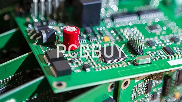
How to process streamlined PCB to improve manufacturing?
Expensive and complicated discrete interconnection cables can reduce a design's reliability, increase design cost and overall design size. Fortunately there is an alternative in the form of flexible and flex-rigid PCBs. Flexible PCBs can provide you with a cost effective and convenient solution to your design's interconnection requirements, with the added advantage of having the repeatability and reliability of a PCB. Whereas discrete interconnections have inherently different conductor orientations, flexible PCBs hold all conductors in fixed special orientations to each other.
This consistency of composition allows for the precise modeling of flexible PCB traces and a more predictable design. Additionally, flexible PCBs can include gold finger contacts allowing for the edge of a flexible PCB to serve as the male portion of a connector and can accommodate high density designs. As such flexible PCBs can be used to replace the vast majority of traditional discrete interconnection solutions while still allowing for a highly modular design.
Beyond providing an efficient means of producing an interconnect solution for a design, flexible PCBs can also accommodate components and be the basis for an entire solution. Using a flexible PCB in place of a traditional PCB can allow for smaller and less conventional PCB designs that are able to fit in housings that would otherwise not be able to accommodate a traditional PCB. Instead of mounting your components to a rigid PCB you can mount then on a flexible solution and they will conform to contoured housings.
Furthermore, portions of a flexible PCB can be stiffened with a stiffening substrate to increase the reliability. Finally, flexible PCBs lend themselves to the lightest possible solution, as flexible PCBs are significantly lower in weight per unit area compared to traditional PCBs. Examples of applications that are commonly based on a flexible PCB solution include wearable, digital cameras, medical devices and other small consumer electronics devices.
Flexible PCBs also provide the advantage of being inherently resistant to vibrations. They are often used in automotive devices because of its inherent resistance to vibrations, also well suited to electronics with mechanical components. As such, they are widely used in printers, hard disks and keyboards.

What are the common problems of streamlined PCB components placement?
PCB components that are not placed correctly in a layout can cause problems when the board is being assembled by a contract manufacturer. Incorrectly placed components may not solder correctly, which can result in a host of reliability problems. For example, shorts may be introduced, causing failure of the circuitry. And, the board may have difficulty going through some or all of the automated manufacturing processes.
If not addressed prior to production, component placement issues can lead to delays, or even stop the board from being manufactured. In addition to the immediate manufacturing delays, there could also be a ripple effect that creates larger issues for your project, including:
· Time to market for the PCB or the product that it is used in could be delayed.
· Quality issues could result in reduced confidence in the design.
· There could be an inability to push the design forward into high-volume manufacturing.
· More resources could be required to support design changes.
· PCB or project funding could be jeopardized.
For designs that have not been optimized during the design phase, finding and resolving the issues that can cause immediate manufacturing problems will require more engineering time on both the part of the designer and the CM. Yet, these corrections are necessary to improve yields, manufacturing cycle times, and reduce quality issues with your PCB.
Industry Category


