What Are the Guidelines of Via Stitching in PCB Manufacturing?
By:PCBBUY 08/29/2024 15:26
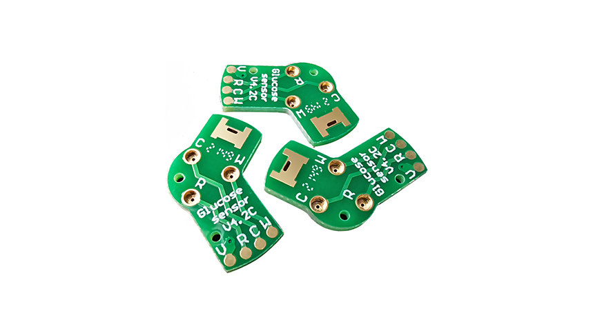
In printed circuit board (PCB) design, via stitching is a vital technique used to connect different layers and ensure signal integrity. It involves the placement of vias in strategic locations to create electrical connections, manage heat dissipation, and mitigate electromagnetic interference (EMI). Via stitching is particularly important in high-frequency and high-power applications, where signal integrity and thermal management are critical. This article will explore the key guidelines for via stitching in PCB manufacturing, including its benefits, types, placement strategies, and design considerations.
1. Understanding Via Stitching in PCB Design
Via stitching involves creating a series of vias (vertical interconnect accesses) that connect copper planes or traces on different layers of a PCB. Vias are essentially small holes plated with conductive material, allowing electrical signals to pass through the various layers of the board. Via stitching provides a low impedance path for signals, reduces noise, and improves the overall stability and performance of the PCB. This technique is particularly useful for reducing electromagnetic interference (EMI) and maintaining signal integrity.
2. Benefits of Via Stitching
Signal Integrity: Via stitching minimizes the return path impedance for high-frequency signals, reducing the potential for signal distortion and improving overall signal integrity.
Thermal Management: By connecting ground planes across layers, via stitching helps distribute heat more effectively, preventing localized hot spots and enhancing thermal dissipation.
EMI Mitigation: Via stitching creates a continuous path for return currents, reducing the loop area and minimizing the risk of electromagnetic interference.
Structural Integrity: Vias add mechanical strength to the PCB, reducing the likelihood of warping or bending under stress.
3. Types of Via Stitching
Ground Plane Via Stitching: This type involves placing vias along the edges of ground planes to ensure consistent grounding throughout the PCB. It helps reduce EMI by providing a continuous grounding path.
Thermal Via Stitching: Used to transfer heat away from components, thermal via stitching involves placing vias in areas with high thermal loads. These vias connect to thermal pads or heatsinks to dissipate heat.
Signal Via Stitching: Used in high-speed designs, signal via stitching ensures that high-frequency signals have a low-impedance path to return currents, reducing noise and signal degradation.
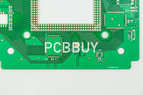
4. Design Considerations for Via Stitching
Via Size and Type
Diameter: The size of the via should be selected based on the current-carrying requirements and the available space on the PCB. A typical via diameter ranges from 0.2 mm to 0.4 mm.
Type: Via types include through-hole vias, blind vias, and buried vias. The choice depends on the PCB stack-up and the specific design requirements.
Spacing and Placement
Edge Stitching: Vias should be placed along the edges of the PCB to connect ground planes effectively. A common practice is to place vias at intervals of 0.5 mm to 1 mm along the edge.
Around Critical Components: Vias should be placed near high-speed components and connectors to provide a low-impedance path for return currents.
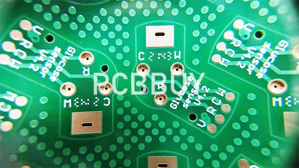
Grid Pattern: For thermal management, vias can be arranged in a grid pattern under components that generate significant heat, such as power transistors or processors.
Electrical Performance
Impedance Control: Vias introduce impedance discontinuities. The placement and size of vias should be carefully managed to minimize impedance variations, especially in high-speed signal paths.
Inductance and Capacitance: The inductance and capacitance introduced by vias can affect signal performance. Via stitching should be designed to balance these effects and maintain signal integrity.
5. Via Stitching in High-Frequency PCB Design
High-frequency PCBs, commonly used in RF (radio frequency) and microwave applications, require precise control over signal paths to prevent loss and distortion. Via stitching plays a crucial role in these designs by providing:
Grounding: Via stitching helps create a low-inductance ground path, reducing EMI and ensuring signal fidelity.
Signal Isolation: Vias can be used to create isolation between different signal paths, preventing crosstalk and signal interference.
Power Integrity: By connecting power planes with vias, via stitching helps maintain consistent voltage levels across the PCB, improving power integrity.
6. Thermal Management through Via Stitching
Thermal management is critical in high-power applications, such as LED drivers, power amplifiers, and CPUs. Via stitching provides an efficient means of transferring heat away from hot components to thermal pads or heatsinks.
Thermal Vias: These are typically larger in diameter to allow more heat to pass through. A common practice is to use multiple thermal vias under heat-generating components to distribute heat more evenly.
Copper Pour and Thermal Pads: Vias can connect copper pours or thermal pads to inner layers or external heatsinks, enhancing thermal conductivity.
7. EMI and EMC Considerations in Via Stitching
Electromagnetic interference (EMI) and electromagnetic compatibility (EMC) are major concerns in PCB design. Via stitching helps address these issues by:
Reducing Loop Area: By connecting ground planes with vias, the loop area for current return paths is minimized, reducing EMI.
Shielding: Vias can be used to create shielding around sensitive signal lines, providing a barrier against external electromagnetic fields.
Filtering: By strategically placing vias, designers can create filtering effects that reduce high-frequency noise.
8. Simulation and Testing for Via Stitching
Before finalizing a PCB design, simulation tools should be used to analyze the effects of via stitching on signal integrity, thermal management, and EMI.
Electromagnetic Simulation: Tools like HFSS (High-Frequency Structure Simulator) can model the electromagnetic behavior of via stitching.
Thermal Analysis: Thermal simulation software can predict the temperature distribution across the PCB and optimize via placement for heat dissipation.
Signal Integrity Analysis: Simulation tools can analyze how via stitching affects signal integrity, helping to optimize via placement and size.
9. Guidelines for Effective Via Stitching
Determine the Via Size and Type: Choose via sizes that balance manufacturing capabilities, electrical requirements, and thermal performance.
Optimize Via Placement: Place vias near critical components, along edges, and in grid patterns for thermal management.
Minimize Impedance Discontinuities: Design vias to maintain consistent impedance in high-speed signal paths.
Use Sufficient Via Density: Ensure enough vias are used to achieve the desired electrical, thermal, and mechanical properties.
Validate Design with Simulation: Use simulation tools to validate the via stitching design before manufacturing.
Consider Manufacturing Constraints: Work with PCB manufacturers to understand their capabilities and limitations regarding via size, spacing, and placement.
Test and Iterate: After manufacturing, test the PCB to ensure that via stitching meets the design requirements and make adjustments as necessary.
Conclusion
Via stitching is a critical technique in PCB manufacturing that enhances signal integrity, thermal management, EMI reduction, and structural strength. By following best practices and guidelines, designers can optimize via stitching to meet the specific needs of their applications. Proper via stitching ensures that PCBs function reliably in high-frequency, high-power, and high-density environments, making it an essential consideration in modern PCB design.
References
1. Hall, S. H., & Heck, H. L. (2000). *Advanced Signal Integrity for High-Speed Digital Designs*. Wiley-IEEE Press.
2. Johnson, H., & Graham, M. (2003). *High-Speed Digital Design: A Handbook of Black Magic*. Prentice Hall.
3. Montrose, M. I. (2000). *EMC and the Printed Circuit Board: Design, Theory, and Layout Made Simple*. Wiley-IEEE Press.
4. Raju, R. (2008). *Practical Guide to RF and Mixed Signal Printed Circuit Board Layout*. Artech House.
Industry Category


