What Are the Key Factors that Affect the ENIG Reaction Mechanism in PCB Manufacturing?
By:PCBBUY 04/23/2024 15:00

ENIG is also called nickel immersed gold, the industry is often called Electroless Nickel Immersion Gold (ENIG), also known as nickel immersed gold.
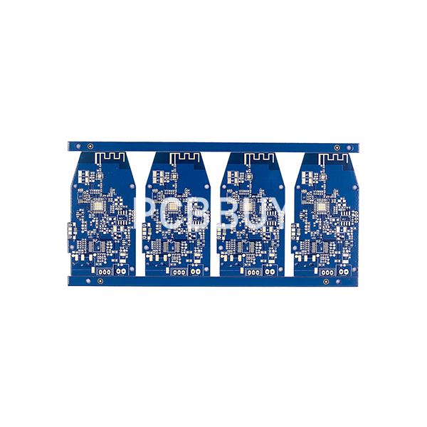
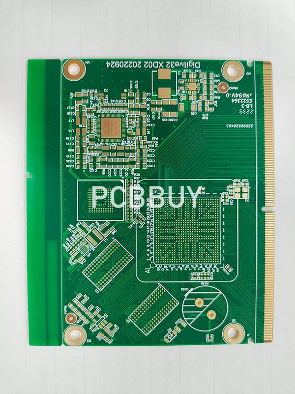
PCB ENIG refers to a solderable surface coating process in which nickel is chemically plated on the surface of bare copper and then chemically dipped gold. It has good contact conductivity, good assembly and welding performance, and it can also be used with other surface coating processes. With the rapid development of the electronics industry, the role of the ENIG process is becoming more and more important. This article mainly introduces the PCB ENIG process flow, the specific follow the small series together to understand.
What Is the Development Background of PCB ENIG?
The background of the development of electroless nickel/gold printed circuit boards, whether single-sided, double-sided or multi-layer structure, are mainly used for the interconnection of electronic components. It is by providing lines and welding parts, so that various components such as resistors, capacitors, semiconductor integrated chips, etc., are now interconnected, so as to become electronic parts with certain functions. Therefore, the PCB board must have a pilot hole, pad or pad. The early wieldable coating is the S-Pb corrosion resistant layer produced by the graphic plating method, which is welded after hot melt to realize the installation of sub-components on the printed circuit board.
Printed Circuit Board Surface Finish Technology
The development of electronic technology requires that the lines and spacing on the PCB become smaller and maintain good reliability, and the bare copper welding resistance film (SMOBC) process masking technology and hot air smoothing process effectively overcome the short circuit problem caused by the traditional hot melt method of narrow spacing lines and the latent short circuit problem under the welding resistance film during wave soldering. However, the high temperature treatment of hot air smoothing will still cause a certain degree of damage to the substrate of the printed circuit board and the surface bending.
At the same time, the surface thickness of Sn-P coating smoothed by hot air varies greatly. The application of surface mount technology (SMT) requires that the connection pad or pad have good coplanality or flatness, while the PCB itself cannot be bent to avoid potential stresses, slippage, collapse and short circuit hazards. Organic weldability protective coating and chemical Ni/Au surface coating can meet the welding requirements of surface mount devices and have been gradually applied. Due to the mass production of mobile phones, tablet computers, electronic watches, financial chip cards and notebook computers, the requirements for surface coatings are multi-functional, which can not only fuse welding, but also require a variety of lap welding, requiring contact conduction function
And assist with heat dissipation functions, etc., and even require welding, lap, contact conduction, and heat dissipation to be integrated on a PCB. Chemical Ni/Au coatings can in principle fully meet all the above requirements. Among them, electroless plating Ni achieves continuous deposition on the printed circuit board through the self-catalytic characteristics of Ni, and the thickness of the general Ni layer is 5um. Electroless plating Au, in fact, chemically dipped Au, is produced by replacing Ni with Au, and the thickness can usually only be between 0.03 and 0.1um, and the maximum is generally not more than 0.15um, so it can only meet the requirements of fusion welding and gold wire lap welding. In the lap welding, the thickness of the Au layer in the chemical Ni/Au is required to be 0.3~0.5um. Therefore, the Au layer is prepared by the method of autocatalytic reduction of Au. The cost of gold plating is very high, so it is difficult to be widely used.
After developing the chemical Ni/Au surface coating, Anmet has developed an automatic catalytic (electroless plating, coating thickness of 0.1~0.3um) surface coating (directly produced on the surface of Cu), which can replace the chemical Ni/Au as a fusion welding coating. More gratily is the development of chemical Ni/Pd/Au (thickness of 5m/0.5um/0.02um) fully functional surface composite coating, which can replace Au layer above 0.3pm for any form of welding and bonding.
PCB ENIG Process Flow Introduction
1. Basic steps
Degreasing → water washing → neutralization → water washing → microcorrosion → water washing → Preleaching → palladium activation → blowing and stirring water washing → no electric nickel → hot water washing → no electric gold → recovery water washing → post-treatment water washing → drying
This is one of the chemical nickel tank formulas.
Formula characteristics analysis:
a. Effect of PH value: turbidity will occur if PH is lower than 8, decomposition will occur if PH is higher than 10, and there is no obvious effect on phosphorus content, sedimentation rate and phosphorus content.
b. Temperature effect: temperature affects the precipitation rate greatly, the reaction is slow below 70°C, and the rate is fast and uncontrollable above 95°C.90°C is the best.
c. The concentration of sodium citrate is high; the concentration of chelating agent increases, the deposition rate decreases, the phosphorus content increases with the concentration of chelating agent, and the phosphorus content of triethanolamine system can even be as high as 15.5%.
d. The deposition rate increases with the increase of the concentration of reducing agent sodium dihydrogen hypophosphate, but the decomposition of the tank after more than 0.37M, so the concentration should not be too high, too high is harmful. There is no clear relationship between the phosphorus content and the reducing agent, so the general concentration is controlled at about O.1M.
e. The concentration of triethanolamine will affect the phosphorus content and deposition rate of the coating, and the deposition will be slow as the concentration increases and the phosphorus content decreases, so it is better to maintain the concentration of about 0.15M. In addition to adjusting pH, it can also be used as a metal chelating agent
f. It is concluded that the phosphorus content of the coating can be effectively changed by adjusting the concentration of sodium citrate
H. General reducing agents are broadly divided into two categories:
Sodium Hypophosphate (NaH2PO2H2O, Sodium Hypophosphate) series and sodium Borohydride (NaBH4, Sodium Borohydride) series, sodium borohydride is expensive, so the market mainly sodium hypophosphate is generally recognized as:
[H2PO2] -H2OA H [HPO3] 2-2H (Cat)
Ni2 2 h (Cat) a Ni 2 h
[H2PO2] - H (Cat) a H2O OH - P
[H2PO2] -H2Oa H [HPO3] 2-H2
The copper surface is mostly non-activated surface in order to produce electronegativity to achieve "start plating", the copper surface is long before mining without electric palladium reaction has phosphorus eutectoid, so the phosphorus content of 4-12% is common. Therefore, when nickel is much, the coating loses elasticity and magnetism, and the brittle luster increases, which is good for rust prevention and bad for wire and welding.
The chemical N/Au surface coating is a technology of depositing vertical welding heat or welding foot to form a protective layer after the solder resistance layer is made on the printed circuit board. Because the welding pad or welding foot on the printed circuit board after welding is relatively independent, the nickel and gold deposition can only be achieved by chemical method. The thickness of the chemical i/A coating is uniform, and the coplanarity is good, which not only protects the surface, but also protects the side of the welding pad or welding foot.
As a PCB manufacturing surface coating, the thickness of the Ni layer is required to be >Sum, while the thickness of the Au layer is 0.05 ~0.1um, and the thickness of the Au layer as a weld able coating cannot be too large, otherwise it will produce brittleness and weak solder joints, and the protection performance of the Au layer is too bad. Since the weldability of the chemical Ni/Au coating is reflected by the Ni layer, Au is only provided to protect the coal bonding of i. Therefore, from an engineering point of view, the success or failure of the chemical Ni/Au process will be reflected in whether the quality of the Ni layer produced meets the requirements of the application.
At present, there are many professional manufacturers to provide chemical Ni/Au manufacturing processes and products, are also on the scale of automatic line, in recent years to enter the Chinese market suppliers Atotech, MacDermid, OMI, LeaRonal, Shipley, on the village and so on. At present, electroless Ni/Au has been widely used in major printed circuit enterprises, and has become an important surface treatment method for SMT pads
What Are the Key Factors that Affect the ENIG Reaction Mechanism?
1. Reaction mechanism
(NaH,PO,), at high temperature (85 ~100C), Ni2+ on the catalytic surface is also electroless ENIG with the help of hypophosphate, which is originally a metal, and this new Ni can be used as a catalyst to continue to promote the reaction. As long as the various factors in the solution are controlled and supplemented (referring to the components), a nickel coating of any thickness can be obtained. This reaction is called "autocatalysis" or "self-catalysis", and no external power supply is required to complete the reaction.
The industrial application of chemical ENIG began after 1964, when Bonet and Littier of the Soviet Union invented the principle of catalytic surface-controlled Ni-P alloys. Electroless ENIG is mostly used for corrosion prevention of products with complex shapes (such as precision parts in the watch industry), improve wear resistance, prevent magnetic adhesion, and prevent high-temperature (500 ~600C) corrosion. It is now used in the printed circuit board manufacturing industry as a Ni/Au coating for corrosion resistance, welding, contact conduction and heat dissipation. Electroless plating can be applied to ferrous metals, copper and copper alloys, aluminium and aluminium alloys, and specially treated plastics.
Electroless ENIG using hypophosphate can only be used directly on certain metals (such as nickel, iron, drill, and aluminum). When nickel is plated on copper and brass and other metals, it is necessary to make them more reactive than nickel. The chemical nickel coating obtained is a Ni-P alloy containing phosphorus below 15%, and the plating solution formula has two types of alkaline and acidic, but the acidic formula is mainly used in the PCB product field
The electrochemical mechanism of electroless ENIG is as follows:
Anode reaction:
H2PO2+ H20→HPO32 +3H+ +2e
Cathode reaction:
Ni2+ +2e→Ni
H2PO2+2H+ +e→P+2H20
In addition, there is a side reaction of H+ reduction to hydrogen gas, the reaction equation is
2H+ +2e→H2
Ni and P of the new ecology:
3Ni+P→Ni3P
2. Influence of various factors on ENIG speed
(1) Temperature
The relationship between reaction rate and temperature of electroless ENIG can be expressed using Arrhenius equation. For endothermic reaction, increasing the temperature can increase the activation energy of Ni-P chemical deposition reaction, and then increase the rate of deposition reaction. The chemical deposition of nickel is a typical endothermic reaction, which can only occur at temperatures above 60C. The electroless ENIG rate increases with the increase of temperature. When the temperature rises from 90C to 100C, the deposition rate of nickel doubles. Alkaline electroless ENIG can be performed at lower temperatures.
(2) pH electroless
Plating can be performed in acidic and alkaline solutions. The pH value is best 5 or high, at which time the nickel speed is 10 ~30um/h. When the pH value is reduced, the plating rate in the acidic solution slows down until the ENIG stops completely.
(3) Nickel salt concentration
When the hypophosphate concentration is low, the change of nickel salt concentration has little effect on the nickel deposition rate. However, if the concentration of nickel salt is increased at the same time as the hypophosphate content, the ENIG speed is accelerated. Therefore, the rate of ENIG depends on the ratio of nickel salt to hypophosphate in the solution. The optimal ratio is generally considered to be 0.4, between 0.25 and 0.6
(4) Additives that have a significant effect on the deposition rate are organic additives:
Glycolic acid, acetic acid, formic acid, citric succinct acid, lactic acid, malice acid, amino acetic acid, amino succinct acid and the salts of these acids. In the reduction process of organic additives, some of them are phosphates that bind nickel to the conjugate and prevent nickel precipitation. The rate of nickel reduction increases to the maximum with the increase of the concentration of organic additives, at which time a smooth and bright coating is deposited.
The above effect is caused by the additive accelerating the decomposition of hypophosphate. On the contrary, some inorganic additives :Cd2+A13+ and CN- can block the ENIG process, while Pb2+ and SCN- can completely stop the ENIG process.
(5) Reaction products
The reaction product of electroless ENIG accumulates and enters the sediment, causing the acidity of the solution to increase and the rate of nickel precipitation to slow down until the ENIG process stops. Even if the salt and hypophosphate are automatically supplemented, the whole solution must be replaced after a certain time.
In order to improve the stability of the solution, the complex is added to prevent the precipitation of nickel phosphite. In alkaline solutions, the complexing agents are ammonia and sodium citrate. Amino acetic acid was used as complexing agent in acidic solution.
Ferric chloride can remove the nickel phosphite in the solution and extend the working life of the bath. Ferric chloride forms an insoluble complex with phosphite, which is easily removed by filtration
3. Composition and structure of chemical nickel coating
The coatings obtained in acidic solution contain P of 7% ~ 10% (mass fraction), and those obtained in alkaline solution contain P of 5% ~7% (mass fraction). The presence of phosphorus determines a series of special properties of the coatings, which change significantly after heat treatment.
As a PCB surface coating, weldability is first and foremost. Nickel coatings for this purpose require a P content of 7% to 9%(mass fraction).
The pH value of the solution is the main factor affecting the P content of the coating. For example, the pH value is reduced from 5.5 to 3.5, and the P content in the alloy is increased from 7.5% to 14.5%, so the pH value of the solution must be controlled, generally in 5.1, and an alloy coating containing about 9% phosphorus can be obtained. The results of X-ray and electron microscopy show that the chemical nickel coating is amorphous and has a layered structure and a super cooled liquid structure.
4. Protective performance of coating
With the different deposition conditions, the electroless ENIG layer has different porosity and corrosion stability. The experimental results show that the chemical nickel layer obtained in acidic solution has fewer pores and higher chemical stability than that obtained in alkaline solution.
5. Physical and mechanical properties of the coating
The micro hardness of the chemical coating is 3.4 ~4.9kN, and it increases with the increase of P content. Heat treatment can increase the hardness and improve the wear resistance.
6. Acquisition of bright chemical nickel layer
Bright chemical nickel layer can be obtained by various methods.
1) Add the same additive to electroless ENIG solution as bright ENIG.
2) Add acetic acid drill 2.S/L or more in the solution, or add 0.3g/L uranium acetate hn a plating area, the larger the area, the brighter the plating.
Reference
He Wei, PCB Basic Electrical Information Science and Technology, China Machine Press,188-191
Industry Category


