What Are the Main Factors of PCB Assembly Drawing?
By:PCBBUY 03/02/2024 16:25

Your fabrication and assembly drawings will communicate different information to the vendors that they are intended for. The fabrication drawing will include information on how the raw printed circuit board is to be built, while the assembly drawing will include details on how the components will be attached to that raw PCB. In either case however, you will start from the same place with these drawings; in your PCB design tools.
Do you know the definition of PCB assembly drawing? If you are going to learn more information of PCB assembly drawing, please check and read the content below for more professional knowledge.
What Are the Main Factors of PCB Assembly Drawing?
An assembly drawing can be made in several forms so as to be the most convenient, and accurate for the manufacturer you work with. Make sure that during your printed circuit board design process you are communicating with your manufacturer to know what they need in their assembly drawings. But while it’s important to keep in mind who you’re working with, here are some basic elements that are common to most printed circuit board fabrication drawings to become familiar with:
Drawing format: Some CAD systems will generate the drawing format for you while others require you to create it as a separate library shape. Whichever method that you use, you will combine that format with your design database to build your drawing.
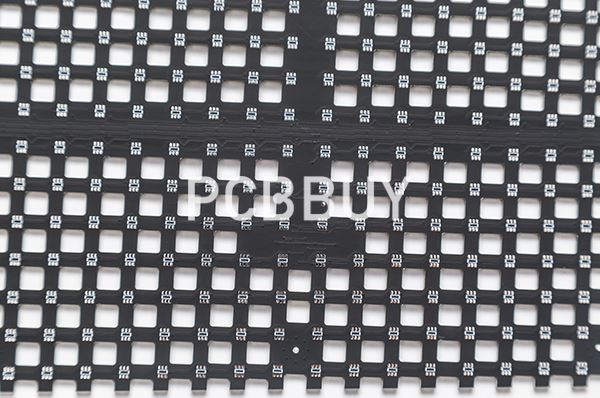
Board outline: As with a fabrication drawing, you will want to display the board outline of your design. Depending on the size of the board, the image can be scaled down to fit the drawing format, or scaled up to show greater detail.

Part shapes: Within the board outline you will want to display all the part shapes and their reference designators that are going to be soldered onto the board.
Mechanical parts: You will also want to display any mechanical parts that will be attached to the board with mounting hardware. Since these parts may not be a regular PCB footprint, you may have to add or draw these shapes separately. An example of this kind of mechanical part is an ejector handle. This is a non-electrical part and may not be represented in the schematic, but it will need to be included on the assembly drawing and in the bill of materials.
Assembly notes: These are a list of instructions that include basic assembly details, references to industry standards & specifications, and locations for special features.
Identification label locations: Any identification labels such as barcodes or assembly tags will need to be located with a drawing pointer and a reference to the specific label in the assembly notes.

Additional views: PCBs that have parts on both sides of the board will usually need a view of the back side of the board in addition to the front. If the board is small enough, both views are sometimes placed on the same drawing sheet. For larger boards additional drawing sheets can be used. You may also need to include a side view of the board to show how certain mechanical parts need to be attached.
What are the considerations of PCB assembly drawing?
A drill chart demonstrates all the particular symbols assigned to the drilled holes in the board outline. This chart contains the information related to the drilled hole requirements of the circuit board to be manufactured. Drill symbols may be shapes or textual characters used to represent a hole’s position. These symbols are generated by the PCB layout software.
A drill chart features specific symbols with respect to the hole size. This chart also displays details about the number of holes of a particular size, whether they are plated or not, what their hole tolerances are, and so on.
Apart from this must-have information, there are other details that can be included in the fab notes section to ease the manufacturing process.
· Controlled impedance requirements: To achieve the desired controlled impedance, trace thickness, trace width, trace distance from the reference planes, and dielectric constant should be varied accordingly. Any basic impedance calculator can be used for this.
· Board manufacturing specifications.
· Designation of the board’s primary side.
· Raw material specification for the boards: These should meet all the required standards.
· Plating details.
· Solder mask and associated specifications (color, finish, etc.)
· Surface finish: If the surface finish is not mentioned in particular, then ENIG is applied on the board.
· Gold fingers: If gold fingers are a part of the circuit board construction, they can be optionally mentioned in the fab drawing.
· All the critical mechanical specifications related to the hole position.
· Presence of via-in-pad/plugged via.
· Implementation of blind/buried via.
· Tolerances:
· Board tolerance (typically ±10%).
· Etching and plating tolerance.
Industry Category


