What Are the Main Types of PCB Electrical Testing?
By:PCBBUY 08/27/2024 16:53
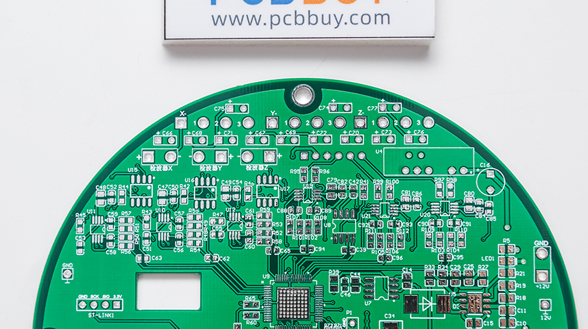
Circuit Boards (PCBs) are fundamental components in modern electronics, serving as the backbone for connecting various electronic components. To ensure their reliability and functionality, PCBs must undergo rigorous testing. Electrical testing is crucial in identifying faults, verifying designs, and ensuring the board functions as intended. This article provides an in-depth exploration of the main types of PCB electrical testing, highlighting their importance, methodologies, advantages, and limitations. We will also include professional data, equations, and tables to provide a comprehensive understanding.
Introduction to PCB Electrical Testing
Importance of Electrical Testing
Electrical testing is vital in the PCB manufacturing process as it ensures the board's functionality before it is assembled into a final product. Detecting faults at an early stage reduces costs, saves time, and prevents potential failures in the field. Common issues detected through electrical testing include:
Short Circuits: Unintended connections between two points.
Open Circuits: Disconnections or breaks in the circuit path.
Incorrect Component Placement: Components not soldered correctly.
Impedance Variations: Deviations in the expected impedance, affecting high-speed signals.
Categories of Electrical Testing
PCB electrical testing can be broadly categorized into two main types: **bare board testing** and assembled board testing.
Bare Board Testing: This is conducted on the PCB before any components are soldered onto it. The goal is to ensure that the board has been manufactured correctly, with no shorts or open circuits.
Assembled Board Testing: This type of testing occurs after the components have been assembled onto the PCB. It ensures that not only the PCB but also the assembled components are functioning correctly.
Types of Bare Board Electrical Testing
Bare board testing focuses on verifying the electrical connectivity of the PCB's conductive pathways. The main types include:
Continuity Testing
Continuity testing checks for open circuits, ensuring that all the connections that should exist are present. A current is passed through the circuit, and if it flows without interruption, the continuity is confirmed.
Methodology: Continuity testing uses a low voltage and current, typically in the range of 1V and 10mA, to avoid damaging the PCB. A multimeter or dedicated test equipment applies a voltage across the points being tested.
Advantages: Simple, quick, and effective for detecting open circuits.
Limitations: Cannot detect short circuits, as it only verifies the presence of a continuous path.
Isolation Testing
Isolation testing ensures that there are no unintended electrical connections (short circuits) between different conductive paths that should be isolated.
Methodology: Isolation testing applies a higher voltage (typically 100-500V) across the points to be tested to ensure no current flows between them. The test equipment measures the resistance, which should be infinitely high or within acceptable limits to indicate isolation.
Advantages: Effective in identifying short circuits and ensuring electrical isolation.
Limitations: It can be more time-consuming than continuity testing and may require higher test voltages that could potentially stress the PCB.
Flying Probe Testing
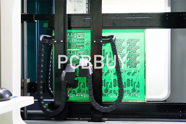
Flying probe testing is a versatile method where one or more probes move over the PCB to test different points for electrical continuity and isolation. It is suitable for low-to-medium volume production.
Methodology: The test probes move over the PCB, testing each point according to the test program. The system compares the actual measurements with the expected values.
Advantages: No need for a dedicated test fixture, making it flexible and cost-effective for small production runs or prototypes. Can detect opens, shorts, and resistance values.
Limitations: Slower compared to fixture-based testing for high-volume production. The accuracy can also be limited by probe alignment.
Bed-of-Nails Testing
The bed-of-nails test uses a fixture with numerous pins (nails) that contact the test points on the PCB simultaneously. This method is highly effective for high-volume production.
Methodology: The PCB is placed on the bed-of-nails fixture, and the pins contact the test points. A test program applies signals to specific pins while measuring responses at other pins to verify continuity and isolation.
Advantages: Fast and suitable for high-volume testing. High accuracy due to fixed alignment of the test points.
Limitations: Expensive to design and manufacture the fixture, making it less suitable for low-volume production or frequently changing designs.
Types of Assembled Board Electrical Testing
After the PCB has been populated with components, it undergoes assembled board testing to verify the functionality of the entire assembly.
In-Circuit Testing (ICT)
In-circuit testing checks the electrical performance of individual components on the PCB and the integrity of the solder joints. It is one of the most comprehensive testing methods for assembled PCBs.
Methodology: ICT uses a bed-of-nails fixture to contact test points on the PCB. The test equipment applies signals and measures responses, checking for correct values of resistance, capacitance, and other parameters.
Advantages: Provides a thorough check of the PCB, detecting a wide range of faults including component values, shorts, and opens. Automated testing offers high throughput.
Limitations: High setup cost due to the need for a custom fixture and test program. Not suitable for high-frequency testing due to parasitic effects from the test fixture.
Functional Testing
Functional testing verifies that the assembled PCB functions correctly within its intended environment. It simulates the operating conditions of the final product.
Methodology: The PCB is powered up, and various inputs are provided while monitoring the outputs to verify correct functionality. This can include running software diagnostics or connecting to other equipment to simulate real-world usage.
Advantages: Ensures that the PCB works as intended, providing a high level of confidence in product reliability. Can detect faults not found by ICT, such as timing issues or incorrect firmware.
Limitations: Requires detailed knowledge of the product's operation, which can complicate the test development process. Slower than ICT due to the need for full functional verification.
Boundary Scan Testing
Boundary scan testing, based on the IEEE 1149.1 standard (also known as JTAG), is used to test the interconnections between integrated circuits on a PCB.
Methodology: Boundary scan involves adding test logic to the ICs, which allows for the testing of interconnects without physical probes. The test logic can shift data into the ICs, drive pins, and read back the results.
Advantages: No need for physical test access to the PCB, making it suitable for densely packed boards with limited test points. Can test for both manufacturing defects and functional faults.
Limitations: Only applicable to ICs with boundary scan capability. Limited coverage for analog components or non-JTAG-compliant devices.
Flying Probe Testing (Assembled Boards)
Flying probe testing can also be applied to assembled PCBs, particularly for low-volume production or prototypes.
Methodology: Similar to bare board flying probe testing, but adapted to accommodate components. The probes test for component presence, orientation, and basic functionality.
Advantages: Flexible and low setup cost. Suitable for complex boards with limited test access.
Limitations: Slower than ICT and may not provide as thorough a test coverage for complex functional verification.
Advanced Testing Techniques
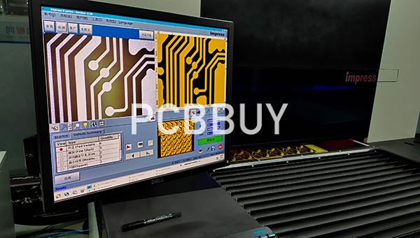
Automated Optical Inspection (AOI)
While not an electrical test, AOI is frequently used alongside electrical testing to inspect solder joints and component placement visually.
Methodology: AOI uses cameras and image processing to inspect PCBs for defects such as missing components, incorrect placements, and solder joint issues.
Advantages: Fast and non-contact. Provides high-resolution inspection for detecting visual defects.
Limitations: Limited to visual inspection; cannot detect electrical faults. False positives can occur due to image recognition errors.

X-ray Inspection
X-ray inspection is used for inspecting hidden solder joints, such as those under Ball Grid Array (BGA) packages.
Methodology: X-rays penetrate the PCB, capturing images of internal solder joints. These images are analyzed to detect solder voids, misalignment, and other issues.
Advantages: Non-destructive inspection of hidden joints. Can detect defects that are invisible to optical inspection methods.
Limitations: High equipment cost and slower than optical inspection. Requires skilled interpretation of X-ray images.
Data and Analysis
Test Coverage Metrics
To evaluate the effectiveness of PCB testing, various metrics are used to quantify test coverage. Table 1 provides a comparison of test coverage for different electrical testing methods.
|
Testing Method |
Testing Method |
Testing Method |
Testing Method |
Cost |
|
Continuity Testing |
50 |
Low |
Fast |
Low |
|
Isolation Testing |
50 |
Low |
Fast |
Low |
|
Flying Probe Testing |
85 |
Medium |
Medium |
Medium |
|
Bed-of-Nails Testing |
95 |
High |
High |
High |
|
In-Circuit Testing |
99 |
High |
High |
High |
|
Functional Testing |
90 |
Medium |
Slow |
Medium |
|
Boundary Scan Testing |
70 |
Medium |
Fast |
Low-Medium |
Equations for Fault Detection
To understand the probability of fault detection, consider the following equation:

This indicates a 99.9% probability of detecting the fault after three independent tests.
Conclusion
PCB electrical testing is critical to ensuring the reliability and performance of electronic devices. Various testing methods, including continuity testing, isolation testing, flying probe testing, and bed-of-nails testing, offer different levels of coverage, cost, and suitability for various production volumes. Advanced techniques such as in-circuit testing, functional testing, and boundary scan testing provide comprehensive verification of assembled boards. Selecting the appropriate testing methods depends on factors such as production volume, PCB complexity, and specific application requirements. As technology advances, new testing methodologies and tools will continue to evolve, enhancing the ability to detect and prevent faults in PCBs.
References
1. Williams, T. (2015). *EMC for Product Designers*. Newnes.
2. Bossert, R. (2003). *Printed Circuit Boards: Design and Technology*. McGraw-Hill.
3. Roberge, J. (2017). *Practical Electronics: A Complete Introduction*. Teach Yourself.
4. Montrose, M. I. (1998). *Printed Circuit Board Design Techniques for EMC Compliance*. Wiley.
5. Johnson, H. W., & Graham, M. (1993). *High-Speed Digital Design: A Handbook of Black Magic*. Prentice Hall PTR.
Industry Category


