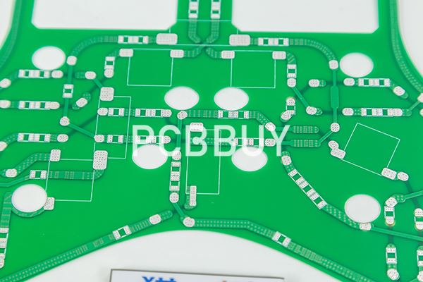
What Are the Main Types of Tests in PCB Manufacturing?
By:PCBBUY 11/15/2023 16:17

Testing is a crucial part of the development cycle for PCBs. When PCB testing is conducted throughout the production cycle, it can help save money and prevent issues when it comes to the final production run.
Some design analysis techniques can be used during the early stages to help minimize major issues during the manufacturing process, but there’s also a wide range of PCB testing methods that can be used on physical boards. These tests, run on prototypes or small-scale assemblies, look most closely at potential shorts, solder joint issues and functionality, ensuring that each tested PCB will function as intended.
Do you know the design for testability guidelines in PCB manufacturing? If you are going to learn more professional knowledge about testability guidelines in PCB, please check and read the content below for more in this passage.
What are the advantages of PCB testing?
Many companies see PCB testing as an absolute must due to the many advantages it provides them. Check out some of the following top advantages of PCB testing:
Increased safety
Since PCBs are often used in essential electronic technologies, their failure can cause major issues for a company’s productivity or an organization’s ability to perform essential services. A defective PCB could cause a fire, potentially putting those near it in danger.
Time savings
PCB testing in the early stages can help save time in the long run, allowing designers to identify major issues during the prototyping stage. Thorough testing enables designers to determine the root cause of each problem posed quickly and easily, making adjustments so that they can move on with production at a faster rate and reduce product lead-time.
Cost reduction
PCB testing prevents wasteful production of faulty products by using prototypes and small-scale assemblies to test the products. By completing thorough testing early in the design process, designers can prevent wasteful full-scale assemblies of faulty PCBs, ensuring that the design is as flawless as possible before it goes into production.
What Are the Main Types of Tests in PCB Manufacturing?
Quality Assurance Testing
The electrical testing methods utilized by CMs can be classified by purpose. Tests conducted to measure your board’s connectivity fall under quality assurance or control. These quality checks may include:

· Impedance testing is performed to ensure there are no open circuits along traces or breaks between soldered connections.
· Continuity testing is done primarily to test the direction of current flow through components, such as diodes.
· Invasive tests, such as sawing, are employed to inspect the board’s internal structure (e.g. layers, vias).
· Most CMs utilize manual or automated inspections as part of their QA regimens. To have any of the above testing methods performed, a request may be necessary. However, none of the above tests require any dedicated design activity prior to manufacturing.
Design for Testability (DFT)
DFT, as the name implies, does require specific design actions to be performed before it can be applied during the manufacturing stage of product development. This generally means adding test points to the board such that parameters of interest can be calculated or measured for direct determination. There are basically two tests that fall under DFT: the flying probe test and the bed of nails test.
Flying Probe Test
The flying probe test is a non-invasive in-circuit test (ICT) to measure open/short circuits, values for passive components and continuity. This test is designed to be applied for prototypes and low production runs. Utilizing the flying probe test is a joint activity that requires the following steps by the PCB designer and CM:
What are test points and test structures?
Since thermal expansion is so important in any PCB that will be repeatedly thermally cycled, you’ll need to determine by how much conductors in your board will expand during cycling. As a board is brought to a high temperature, the substrate and conductors expand, but they can expand at different rates. FR4 substrates experience greater expansion than copper, which puts stress on conductors. Traces on a board are less susceptible to failure as they are sufficiently thick.

In FR4, the thermal expansion coefficient (CTE) increases once the board’s temperature rises above the glass transition temperature. It is always best to use a high-Tg laminate if your board will run at a high temperature as you want to stay below the glass transition temperature.
Simulating microcrack accumulation during repeated thermal cycling is not a simple problem, and simulating this directly is a complex random-walk problem in a random system. However, In general, when the difference between the extreme temperatures is smaller, the board can withstand more cycles.
Industry Category


