What Are the Medical Device PCB Design in PCBA Process?
By:PCBBUY 11/18/2021 09:35

Authorities like IPC, ISO, and FDA (Food and drug administration) have released some standards for populated circuit boards used in medical equipment. These guidelines include all the aspects from production to approval. It is mandatory to follow all these regulations during medical PCB assembly to ensure reliability.
If you are going to learn more details about medical device PCB design, please check and read the content below in this passage for professional knowledge.
How to prototype medical device PCB?
To ensure successful product launch, we offer design and engineering assistance to our medical device customers. This is particularly important because not only must we deliver the prototypes quickly, but they must be manufacturable in volume using the same processes that were used to manufacture the prototype. Those who are experienced with rigid PCBs, flex circuits and rigid-flex designs for medical devices understand that a change in processes or materials can cause a product launch delay due to having to resubmit paperwork or potentially even new samples.
Our job is to work with our customers at the design levels to ensure that when we encounter design challenges like working with very thin dielectric materials, materials with dissimilar X/Y dimensional stability, or very fine line requirements that the PCB can meet the quality requirements such as IPC Class II or III along with the customers testing protocols. Our team of mechanical, electrical, process, CAD, and layout engineers invest the time with our customers so that we can provide optimized manufacturing yields and cost reduction.
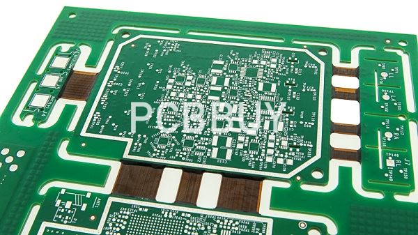
What are the technologies of medical device PCB?
As the technology of medical devices continues to advance, we see the PCBs containing one or more of the following PCB technologies:

IPC Class III:
The biggest issue here is reliability as the 3 biggest factors of the specification.
· The PCB can have no annular ring breakout.
· It must have a minimum of 1 mil of plating in the though holes.
· Tighter tolerances on conductor spacing and widths.
What are the standards of manufacturing medical device PCB?
Medical gadgets and equipment go through more stringent rules and regulations than other electronics. This is because the failure of medical products to function appropriately can cause detrimental impacts, like loss of human life. Thus, each phase of healthcare electronic development undergoes mandatory regulatory oversight to guarantee the best quality and accuracy of the end products.

Medical electronics go through a clear quality management system (QMS) to detect and remove any errors. Acquiescence with such standards is confirmed via various testing routines. The common medical electronic manufacturing standards include:
· The FCC Title 47 rules: These guidelines are made and printed by the Government Printing Office (GPO).
· The Food & Drug CFR Section 807: The FDA’s Center for Devices and Radiological Health (CDRH) regulates companies producing, repackaging, re-labeling, and dealing with medical electronics in the US.
· IEC 60601-1: This guideline outlines the standard aspects of medical electronics.
· IEC 61010-1:It stipulates the standard safety guidelines for electrical equipment and related components.
· IPC 6011: These are basic performance specifications for PCBs.
· ISO 13485 Medical Equipment: This standard is meant for businesses and persons dealing with the design, manufacturing, installation, and servicing of healthcare equipment and gadgets. In addition, certification agencies can use it in their auditing practices.
· ISO 14971:2007: This standard outlines the due process for medical electronic manufacturers to detect any hazard in medical devices.
Remember to design for medical device PCB
You’re placing components and meticulously routing, routing, and re-routing. After that, you’re re-routing some more. While you’re paying attention to a myriad of minutia, it’s easy to forget the things that are most obvious to the people who will actually be assembling, taking apart, and re-assembling your device (even though it’s entirely likely that you’ll be one of them). Are your connectors arranged so that a human hand can reach into the assembly and mate them to their cables? Do pads connected to ground fills have thermal relief connections to ease solderability? Have you exported a 3D model of your board to do a virtual test fit in the assembly? Where are your components placed?
My biggest serviceability nightmare was when I made the mistake of using screw terminal blocks for several connectors. This saved time in initial assembly (no crimping!), but meant that every time the board was removed for debugging, every terminal had to be unscrewed. Every time this happened, I wished I’d just crimped together some cables and used Molex connectors (or anything other than terminal blocks).
Industry Category


