What Are the PCB Troubleshooting And Defect Analysis?
By:PCBBUY 04/28/2022 10:19

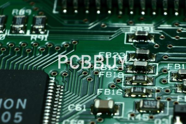
Printed circuit boards, or PCBs, are a mass of insulators and copper traces that connect densely packed components to create a modern circuit. Troubleshooting PCBs is often a challenge, with factors such as size, number of layers, signal analysis, and types of components playing a large role.
Some more complicated boards require specialized equipment to properly troubleshoot. However, most troubleshooting can be done with basic electronic equipment to follow traces, currents, and signals through the circuit.
Are you a beginner of PCB industry? Do you know how to improve the manufacturing process? Please check and read the content below for more professional information.
How to process PCB troubleshooting?
The troubleshooting techniques we’ll see shortly are applicable on single layers, rigid/flex, digital analog, and radio frequency PCBs. But first, you’ll need to map out a PCB. This requires you to develop a clear understanding of its traces, signals, and current flow. Plus, you need to have the knowledge of which capacitor-resistor pairs are ideal to proceed with troubleshooting.
It will also help if you have a good grip on the filter, chole, and voltage divider position in the circuit board. However, suppose you don’t have a solid understanding of the configuration. In that case, it’s ideal to start the troubleshooting process from the connectors – the interface through which erroneous external inputs make their way into the circuit board. That said, you have to be good at mapping a PCB to continue without accessing the board’ schematics. This could eat up a lot of time, as every solder joint will need to be tested using a multimeter probe.
A better, more natural way to trace out PBCs is to use an aluminum piece. This method enables you to search for connections over a broader area per time, reducing the amount of effort and time involved. The process requires a piece of aluminum foil, a wire cutter, crocodile wire clips, and multimeter.
What are the defects for PCB troubleshooting?
The following methods are used in identifying PCB defects and failures:
Identifying failure locations
Failure locations are identified through a variety of devices and techniques, including spectroscopy, microtomography, and micro thermoåcgraphy.
Understanding failure locations
To correctly understand the physical properties of microscopic structures, they are observed using a transmission X-ray microscope, CT scanner, electron probe micro analyzer (EPMA), or other instruments.
Observing and analyzing defective areas
To identify specific causes, defects are closely analyzed through cross-section observation of defective areas, which uses tools such as microscopes, scanning electron microscopes (SEMs), focused ion beam (FIB) microscopes, and EPMAs.

What are the main types of PCB troubleshooting?
Printed circuit boards can cover a single task or multiple functions. PCBs come in three major types:
Single-sided
Double-sided
Multilayer
The electronics industry drives toward more miniaturization, requiring design engineers to produce faster, smaller — and more complex — circuit board technology, which has a higher quality and costs less.
It is important for a printed circuit board to perform its function and support the larger electronic device. Consequently, PCB manufacturers must have a system in place that monitors and tests each component to ensure that it meets various standards and delivers maximum performance.
When a component fails, analysts must utilize various processes, tools and techniques. With accuracy, they must determine why the device failed and how to prevent future failures. The following processes present unique challenges for electronics failure analysis:

Increased density
Higher lead-free process temperature requirements
Hazardous material
Recycling requirements
The need to tune PCBs to precise values
Other associated changes in PCB manufacturing
Root Cause Analysis
The fabrication of a complete PCB assembly requires an array of machines and materials, which include:
Screen printers
Conveyors
Pick-and-place systems
Reflow ovens
Automated optical inspection
Solder paste
Different components
Some machines have automated features that perform checks at various points, and operators perform visual inspections before, during or immediately after the completion of a task.
Nonetheless, many PCBs will fail the final test. When a problem does occur, it is important to perform an effective electronics failure analysis in order to obtain clear and precise details about the source of the problem — and to ensure that it does not happen again.
Industry Category


